
Synchronous semiconductor memory device having a desired-speed test mode

a technology of synchronous semiconductor and test mode, which is applied in the direction of measurement devices, digital storage, instruments, etc., can solve the problems of inability to perform the test according to the desired specification, the time interval between inputs of the commands cannot be controlled, and the total test time cannot be reduced, so as to achieve the effect of not increasing the time length needed for the memory tes

Inactive Publication Date: 2005-03-15
LONGITUDE SEMICON S A R L
View PDF5 Cites 13 Cited by
  • Summary
  • Abstract
  • Description
  • Claims
  • Application Information

AI Technical Summary

Benefits of technology

Enables a low-speed memory tester to perform high-speed tests on high-speed semiconductor memory devices without increasing the total test time, allowing for consistent testing across different memory devices with varying performance specifications.

Problems solved by technology

In this technique, however, the total test time cannot be reduced because these commands are supplied in synchrony with the low-frequency clock signal and a specified number of commands must be supplied to the memory device for the test.
However, in this technique, the time interval between inputs of the commands cannot be controlled, as a result of which the test cannot be performed according to the desired specification.

Method used


Image

  • Synchronous semiconductor memory device having a desired-speed test mode
  • Synchronous semiconductor memory device having a desired-speed test mode
  • Synchronous semiconductor memory device having a desired-speed test mode

Examples


Embodiment Construction

Now, the present invention is more specifically described with reference to accompanying drawings, wherein similar constituent elements are designated by similar reference numerals throughout the drawings.

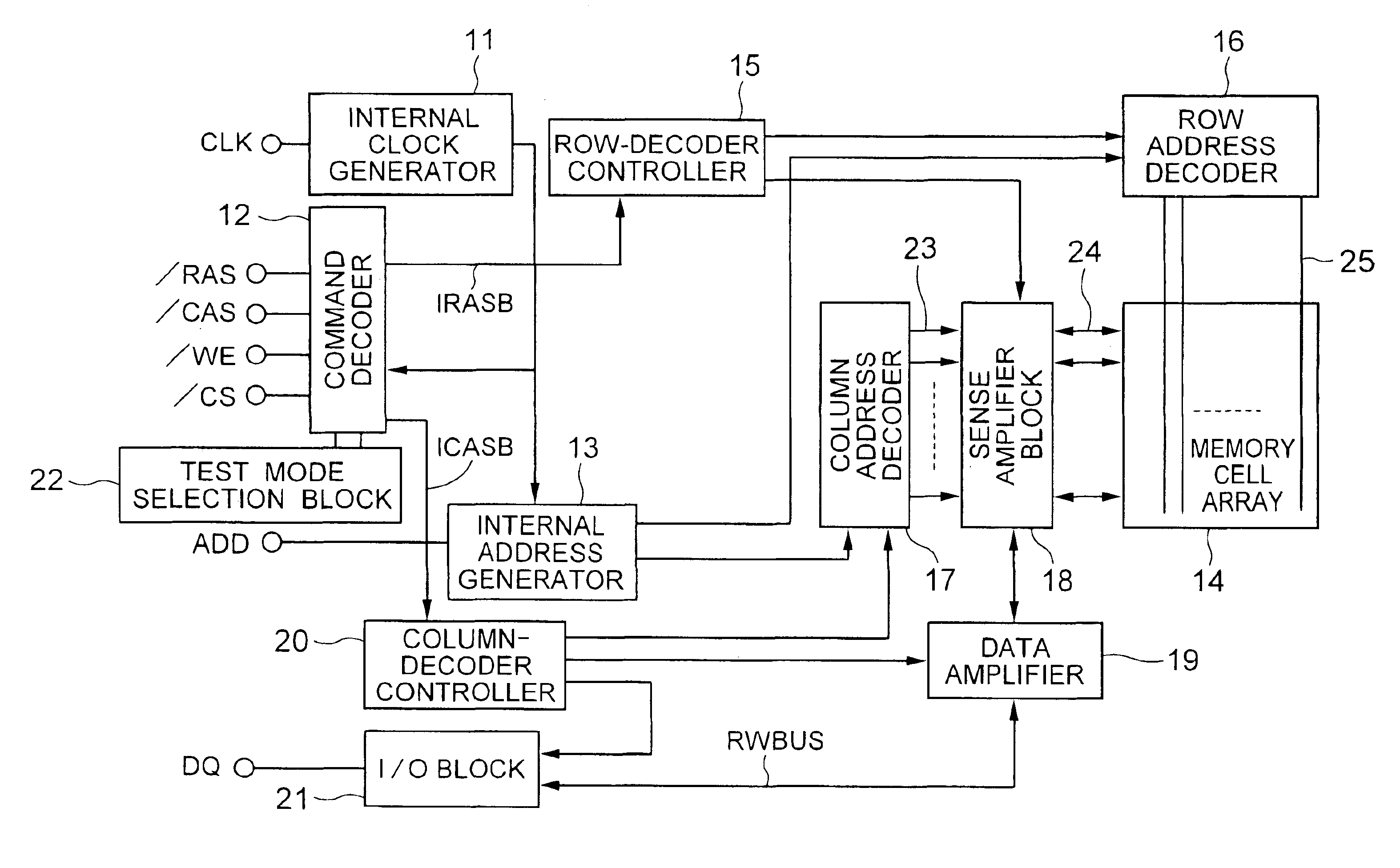
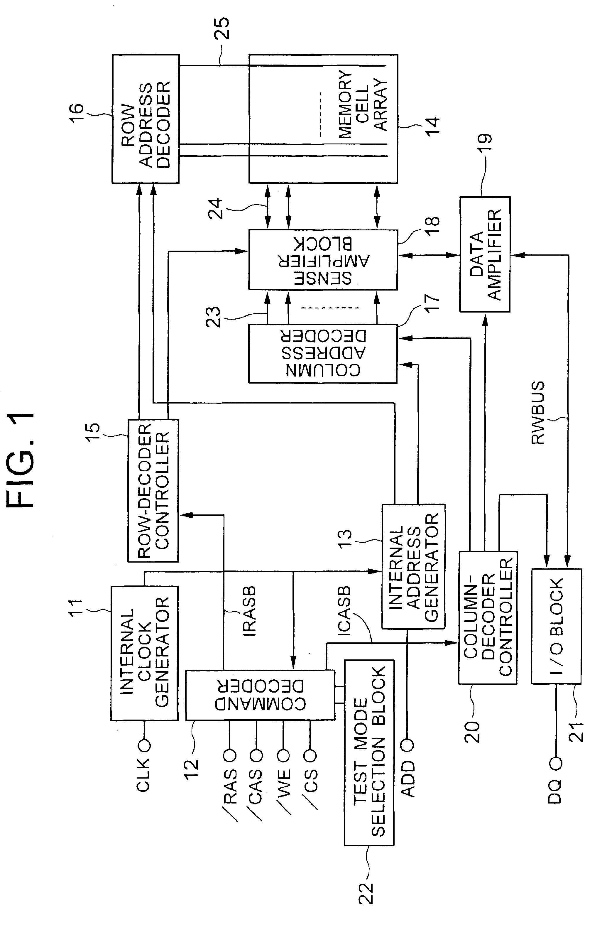
Referring to FIG. 1, a semiconductor memory device according to an embodiment of the present invention is implemented as a SDRAM. Basically, the SDRAM of the present embodiment is different from the conventional SDRAM in that the SDRAM of the present embodiment includes a test mode selection block (mode selection circuit) 22 and performs a different operation during a test mode, as will be detailed hereinafter.

The SDRAM device of the present embodiment includes internal clock generator 11, command decoder 12, internal address generator 13, memory cell array 14, row-decoder controller 15, row address decoder 16, column address decoder 17, sense amplifier block 18, data amplifier 19, column-decoder controller 20, input / output (I / O) block 21, and test mode selection block 22.

The inter...


PUM


Abstract

A synchronous DRAM has a test mode wherein a specified external signal is input to a command decoder of the DRAM. The command decoder generates a plurality of internal commands including activating signal for selecting a word line, write signal, precharge signal, another activating signal and read signal at consecutive timings which do not depend on an external clock signal. A low-speed memory tester can be used for testing the high-speed synchronous DRAM.

Description

BACKGROUND OF THE INVENTION(a) Field of the InventionThe present invention relates to a synchronous semiconductor memory device having a desired-speed test mode.(b) Description of the Related ArtA synchronous semiconductor memory device, such as a synchronous DRAM (SDRAM) device, performs a high-speed read / write operation based on a read / write command which is supplied in synchrony with an external clock signal. FIG. 3 shows a conventional SDRAM device in a block diagram. The SDRAM device includes internal clock generator 11, command decoder 12, internal address generator 13, memory cell array 14, row-decoder controller 15, row address decoder 16, column address decoder 17, sense amplifier block 18, data amplifier 19, column-decoder controller 20 and input / output (I / O) block 21.The internal clock generator 11 receives an external clock signal CLK, to generate an internal clock signal in synchrony with the external clock signal CLK. The command decoder 12 receives external control si...

Claims


Application Information

Patent Timeline
Patent Type & Authority Patents(United States)
IPC IPC(8): G11C29/14G11C29/04G01R31/28G01R31/3183G01R31/3185G11C11/401
CPCG11C29/14G11C29/12015G11C11/401
Inventor AOKI, MAMORU
Owner LONGITUDE SEMICON S A R L
Learn More