
Programmable logic device serial interface having dual-use phase-locked loop circuitry

a serial interface and logic device technology, applied in logic circuits using elementary logic circuit components, logic circuits using specific components, pulse techniques, etc., can solve the problem that some or all of the plls included in the interface may not be used in the user logic design, and the plls are relatively large and complex circuits. the probability of not being used is significant, and the effect of increasing the number of plls

Inactive Publication Date: 2005-03-15
TAHOE RES LTD
View PDF58 Cites 25 Cited by
  • Summary
  • Abstract
  • Description
  • Claims
  • Application Information

AI Technical Summary

Benefits of technology

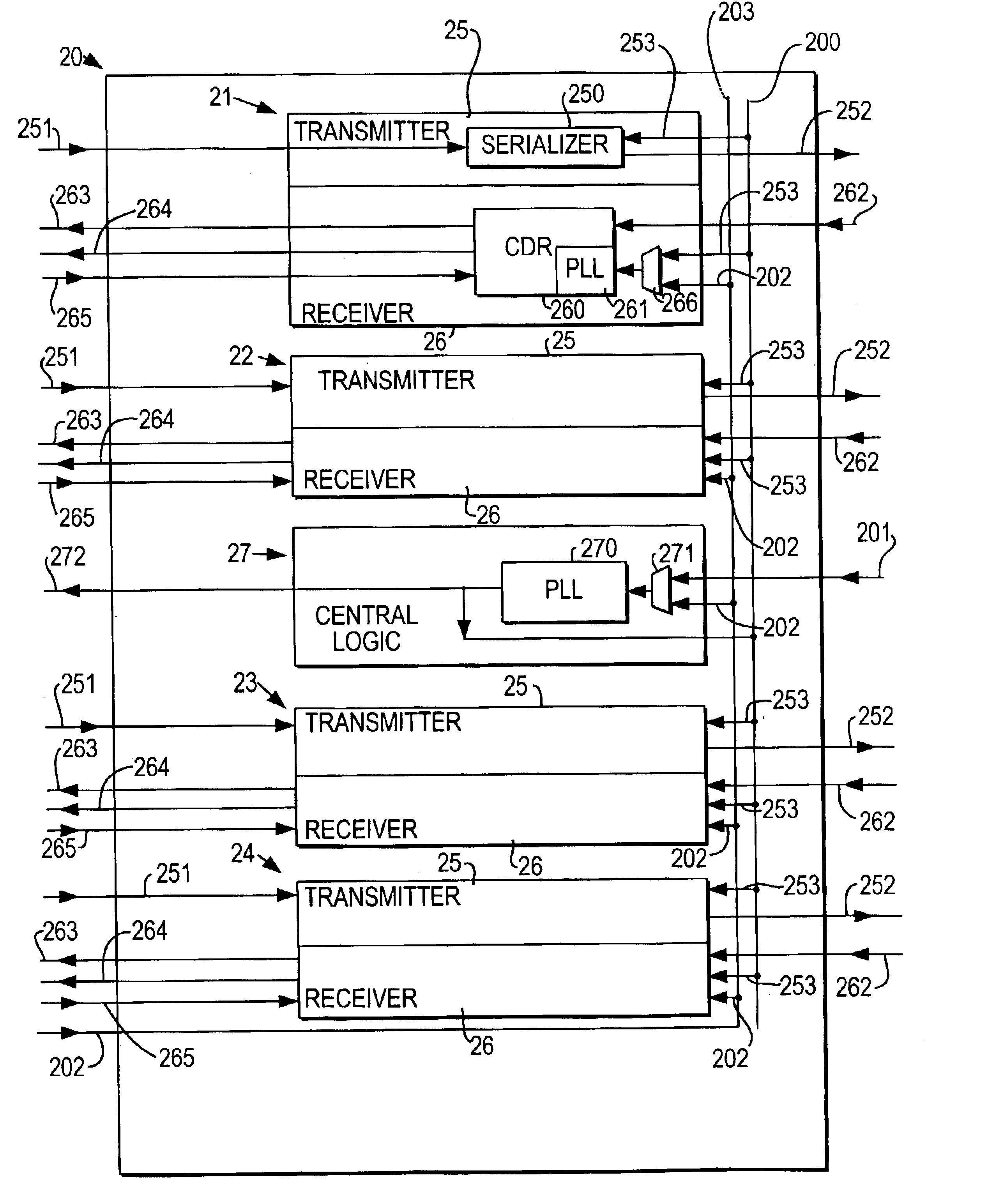
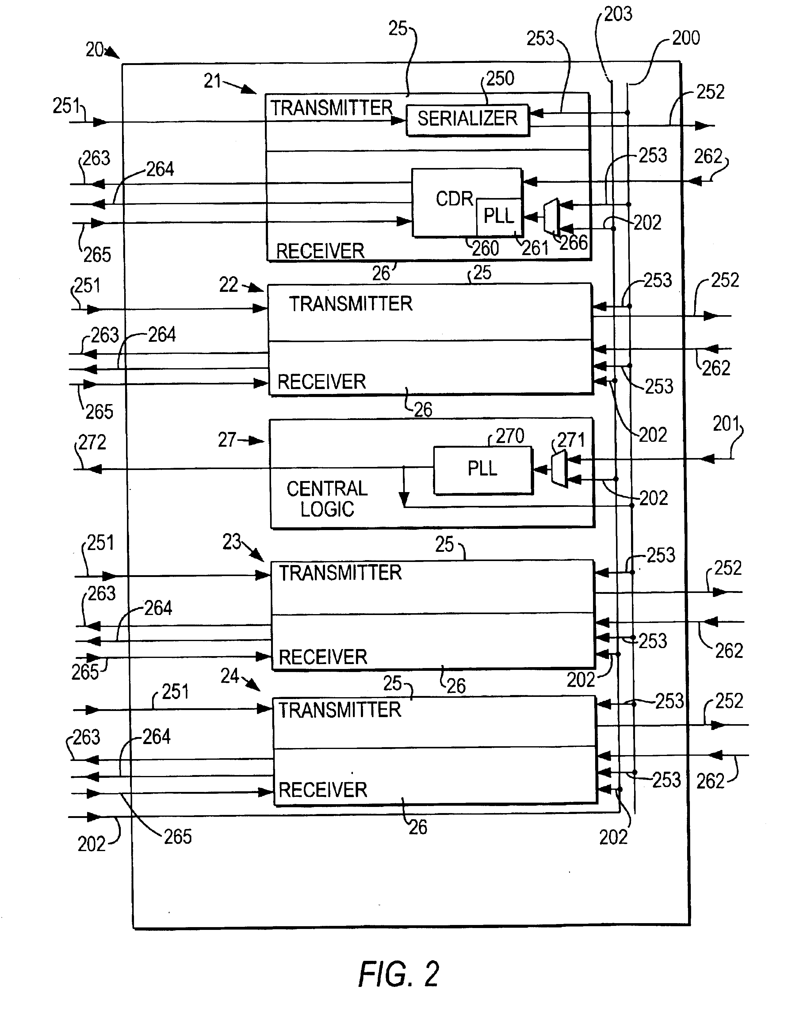
The present invention provides high-speed serial interface circuitry on a programmable logic device that is more flexible than previously known high-speed serial interfaces in that the PLL circuits within the high-speed serial interface can be recaptured when the interface is not being used, or is being only partially used. This is accomplished by providing each PLL in the interface with a first connection that accepts a phase control input from elsewhere on the programmable logic device and a second connection that accepts a reference clock signal either from outside the programmable logic device or from elsewhere on the programmable logic device, instead of from the input serial data for which the serial interface is designed.
Similarly, ordinarily the receiver PLLs receive their reference clock from the input data, while the central logic PLL ordinarily receives its reference clock from either the programmable logic core or off-chip inputs. In accordance with the present invention, each PLL can select its reference clock from either its ordinary source or from a reference clock supplied by the programmable logic core. For example, a multiplexer may be provided that allows a receiver PLL to select as its reference clock either the input data or the core reference clock. A multiplexer also may be provided that allows the central logic PLL to select as its reference clock either an external clock that is provided, or the core reference clock.
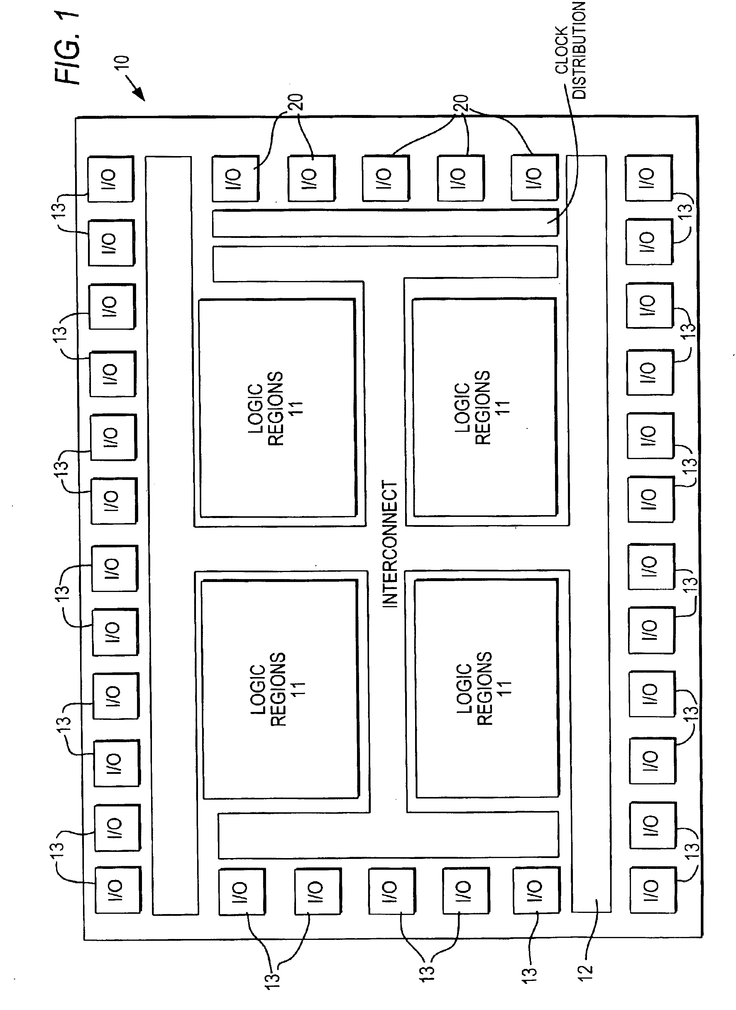
Moreover, although the discussion so far has focused on the multiple PLLs of a single serial interface, a PLD may have several such interfaces and it may be desirable to use the PLLs in more than one interface. If so, it would be preferable for the PLLs in more than one interface to receive the same reference clock signal, and preferably with minimum skew. Therefore, in accordance with this invention there is also preferably provided a multiple interface reference clock distribution network. Such a distribution network preferably includes at least one conductor spanning several interfaces, with each interface, or alternatively each of the PLLs in those several interfaces, being able to be programmably connected to that conductor. More than one conductor may be provided if different groups of PLLs are to be clocked with different reference clocks. And any such conductor or conductors may preferably be arranged as a balanced clock tree or trees to minimize skew in the delivery of the reference clock signals.

Problems solved by technology

PLLs are relatively large and complex circuits, and providing PLLs on PLDs therefore either adds significant area to the PLD, or takes away area that could be used for programmable logic circuitry in a PLD of a given size.
Because PLDs are, by definition, programmable by their users, in any particular user logic design for a PLD including a high-speed serial interface as described above, there is a significant probability that some or all of the PLLs included in that interface may not be used in the user logic design.
As far as that user design is concerned, the PLL circuitry is simply wasted.

Method used


Image

  • Programmable logic device serial interface having dual-use phase-locked loop circuitry
  • Programmable logic device serial interface having dual-use phase-locked loop circuitry
  • Programmable logic device serial interface having dual-use phase-locked loop circuitry

Examples


embodiment 300

One preferred embodiment 300 of a clock distribution network 100 that may be used in accordance with the present invention is shown in FIG. 3. Network 300 is similar to a traditional fully populated PLD switch matrix. Each respective horizontal conductor 301 connects to a respective conductor 203 in one of interfaces 20. At a minimum, there is one vertical conductor 302, having a programmable connection 303 to preferably each one of conductors 301, although three conductors 302 are shown. The actual number of conductors 302 is determined by the number of different core reference clock signals that a user is to be given the capability to use in different ones of interfaces 20. The core-generated reference clock signals preferably are conducted to distribution network 300 on conductors 304. As shown, the number of conductors 304 is equal to the number of conductors 302, but that is not necessary. A fully populated switch matrix 305 is shown connecting conductors 304 to conductors 302....


PUM


Abstract

In a programmable logic device (“PLD”), a serial interface incorporating phase-locked loops (“PLLs”) is provided with connections that allow one or more of the PLLs to be used as general purpose PLLs in the PLD. The connections include conductors to allow reference clock signals from the PLD logic core, or from outside the PLL, to be used by the PLLS, as well as conductors that allow the PLD core to control the phases of the PLLs. For some of the PLLs, conductors to allow the PLL output clock to be used by the PLD are also provided, where such output conductors do not normally exist in such a serial interface.

Description

BACKGROUND OF THE INVENTIONThis invention relates to phase-locked loop circuitry provided in one portion of a programmable logic device, where the phase-locked loop circuitry can be used in another portion of the programmable logic device.It is known to incorporate phase-locked loop (“PLL”) circuitry on programmable logic devices (“PLDs”). For example, it has become common for PLDs to accommodate various input / output (“I / O”) standards, some of which require very accurate high-speed clocks. One way of providing such clocks is to provide PLL circuitry on the PLD.For example, recently PLDs have begun to incorporate high-speed serial interfaces to accommodate high-speed (i.e., greater than 1 Gbps) high-speed serial I / O standards—e.g., the XAUI (10 Gbps Extended Attachment Unit Interface) standard. In accordance with the XAUI standard, a high-speed serial interface includes transceiver groups known as “quads,” each of which includes four transceivers and some central logic. Within each t...

Claims


Application Information

Patent Timeline
Patent Type & Authority Patents(United States)
IPC IPC(8): H03K19/177
CPCH03K19/17736H03K19/17744H03K19/1774
Inventor VENKATA, RAMANANDLEE, CHONG H.PATEL, RAKESH
Owner TAHOE RES LTD
Learn More