Method and apparatus for printed circuit board pads with registering feature for component leads

a printed circuit board and component lead technology, applied in the direction of electrical apparatus construction details, sustainable manufacturing/processing, final product manufacturing, etc., can solve the problems of insufficient adhesive power, limited flexibility in the order of soldering operations, and dislocation of some components, so as to achieve the effect of hardening the solder mound

Inactive Publication Date: 2005-03-15
HEWLETT-PACKARD ENTERPRISE DEV LP
View PDF3 Cites 11 Cited by
  • Summary
  • Abstract
  • Description
  • Claims
  • Application Information

AI Technical Summary

Benefits of technology

Briefly, and in general terms the invention provides a U-shaped metalized pad on a printed circuit board for soldering to a component lead. Solder is disposed on the pad and heated to a molten state so that surface tension and wetting effects form the molten solder into a solder mound having a U-shaped lateral cross section conforming to the U-shaped metalized pad. The solder mound has a first arm and a second arm, and a lateral aperture extending therebetween for receiving an extremity of the component lead. The solder mound also has a bridge portion extending between the first and second arms of the solder mound. The solder mound is cooled so as to harden the solder mound.

Problems solved by technology

It should be understood that flexibility in order of soldering operations is limited since the solder paste on the first side of the circuit board is heated, cooled and hardened before any solder paste is applied to the other side of the printed circuit board.
If solder paste and components were applied to both sides of the printed circuit board before any heat were applied to either side, it is likely that the pull of gravity or vibrations would displace some of the components, since the solder paste has insufficient adhesive power to retain positioning of components so effected.
Flexibility in order of soldering operations is particularly limited when the components include components that must be soldered to pads on both sides of the printed circuit board, such as straddle mount connectors.
Misregistered component leads cause electrically or mechanically defective solder joints, requiring costly and time consuming rework operations.
Misregistered component leads may also cause circuit shorting and catastrophic electrical failure of the entire electronic assembly.

Method used


Image

  • Method and apparatus for printed circuit board pads with registering feature for component leads
  • Method and apparatus for printed circuit board pads with registering feature for component leads
  • Method and apparatus for printed circuit board pads with registering feature for component leads

Examples


Embodiment Construction

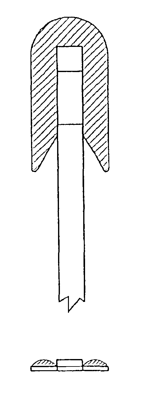
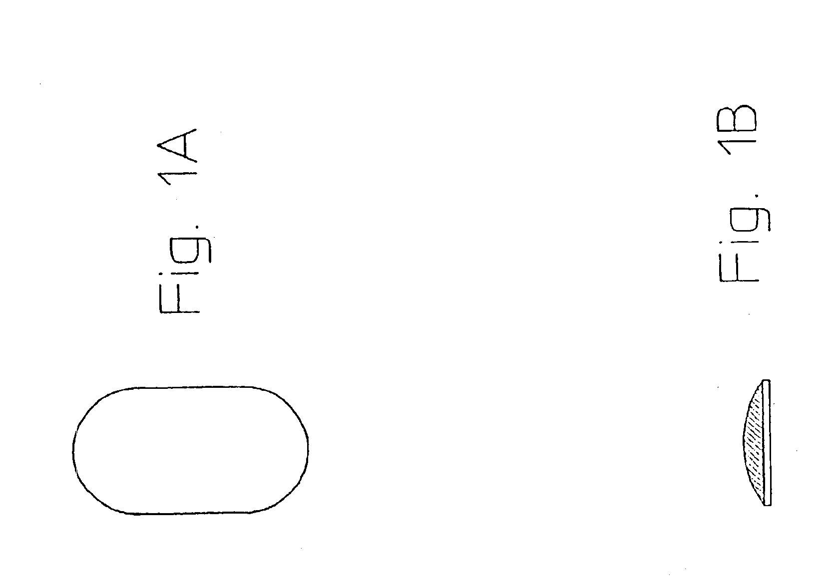
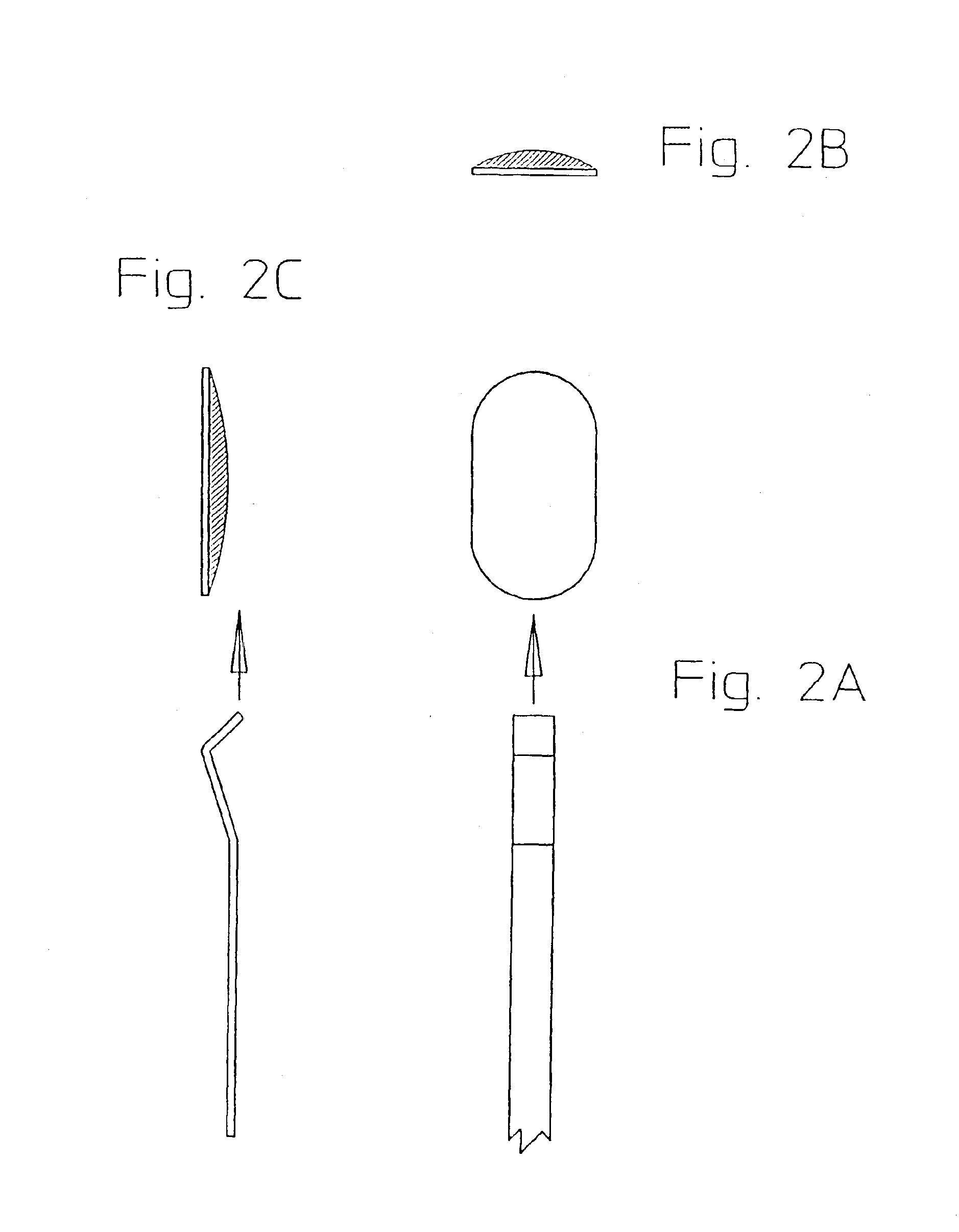
FIGS. 1A, 1B, 2A-C, and 3A-C show various views of solder pad research investigations. In an assembly process, solder paste is placed onto the pads and is melted or “reflowed” into a molten state. A wetting effect spreads the molten solder out to pad edges so as to cover a respective surface of each pad. A surface tension effect causes the molten solder to form a respective solder mound covering each pad, for example as shown in plan view and cross sectional view in FIGS. 1A and 1B. The solder mound is allowed to cool and harden. After component placement on top of the solder mounds, heat is applied to reflow the solder, so as to solder the component leads to the pads.

Leads of each surface mount component are placed onto the tops respective solder mounds of the pads using a combination of motions. In some cases, components are set down onto the board and then pushed laterally using sliding motions across the surface of the board, until leads of each component are in correct lateral ...


PUM

PropertyMeasurementUnit
flare angleaaaaaaaaaa

Abstract

A method and apparatus for printed circuit board pads with registering feature for component leads. A U-shaped metalized pad is disposed on a printed circuit board for soldering to a component lead. Solder is disposed on the pad and heated to a molten state so that surface tension and wetting effects form the molten solder into a solder mound having a U-shaped lateral cross section conforming to the U-shaped metalized pad. The solder mound has a first arm and a second arm, and a lateral aperture extending therebetween for receiving an extremity of the component lead, and registering the extremity of the component lead with respect to the pad.

Description

FIELD OF THE INVENTIONThe present invention generally relates to the field of electronic assembly and more particularly relates to electronic component interconnects in electronic assemblies.BACKGROUND OF THE INVENTIONElectronic assemblies typically employ printed circuit boards for mechanical support and electrical interconnection of electronic components. In the case of surface mount electronic components, component leads are placed onto metal pads deposited onto a surface of the boards. Solder is used to attach the components leads to the pads and to electrically connect the components leads to the pads. The pads are electrically interconnected by traces, or connected to an internal conductive plane of the circuit board through a metal plated aperture extending into the circuit board, called a via, so as to provide for electrical interconnection of the components.In an assembly process, solder paste is placed onto the pads on a first side of the printed circuit board. Components ...

Claims


Application Information

Patent Timeline
Patent Type & Authority Patents(United States)
IPC IPC(8): H01R43/02H05K3/34H05K13/00H05K1/11H05K13/04
CPCH01R43/0256H05K1/111H05K3/3421H05K13/0015H05K13/0465Y10T29/49144H05K1/117H05K3/3405H05K2201/09381H05K2201/09663H05K2201/09709H05K2201/10189H05K2203/043H05K2203/048Y10T29/4913Y10T29/49149H01R43/0263Y02P70/50
Inventor LICHTENWALTER, GUYMARSCHKE, NORMAN D.
Owner HEWLETT-PACKARD ENTERPRISE DEV LP
Why Eureka
Try Eureka