
Method for eliminating noise interference and acoustic noise by printed circuit board ground plane layout

a technology of printed circuit board and ground plane, applied in the direction of electric variable regulation, process and machine control, instruments, etc., can solve the problems of unstable or producing acoustic noise of electronic products, and not being able to have an unstable function, so as to avoid a noise loop and eliminate noise interference and acoustic nois

Inactive Publication Date: 2005-03-08
DELTA ELECTRONICS INC
View PDF5 Cites 8 Cited by
  • Summary
  • Abstract
  • Description
  • Claims
  • Application Information

AI Technical Summary

Benefits of technology

It is an object of the present invention to provide a tree branching technique by a printed circuit board ground plane layout for avoiding a noise loop and further eliminating noise interference and acoustic noise.
It is another object of the present invention to provide a power supply system having multiple outputs which can achieve the purposes of system stabilization and noise interference and acoustic noise reduction without the need of synchronizing the operation frequencies of multiple power converting modules.
It is a further object of the present invention to provide a method for eliminating noise interference and acoustic noise by a printed circuit board ground plane layout, which can be applied for a power supply system having multiple outputs for adjusting the operation frequency of each power converting module so as to reduce cost and increase efficiency.
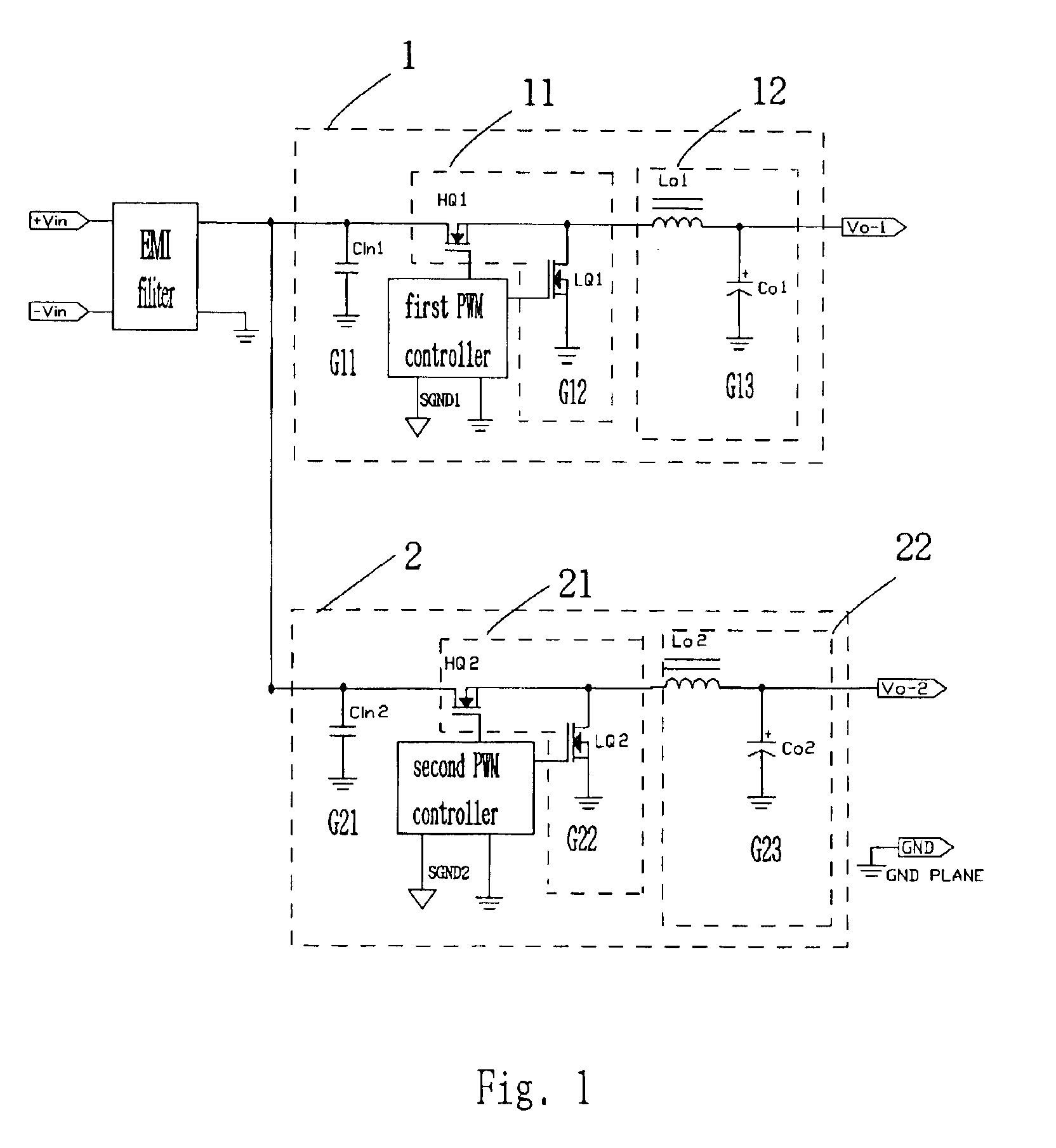
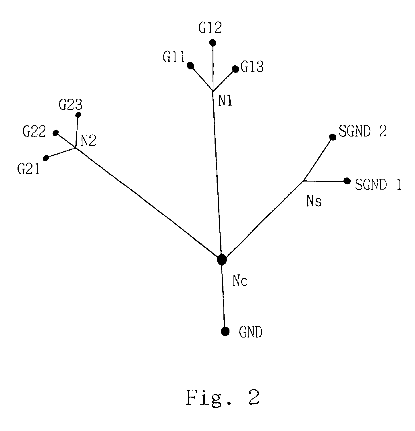
In accordance with an aspect of the present invention, a method for eliminating noise interference and acoustic noise by a printed circuit board ground plane layout applicable to a circuit system having multiple outputs, wherein the circuit system has a first power converting module, a second power converting module and a printed circuit board, and the first power converting module and the second power converting module respectively includes a first ground pin group and a second ground pin group, the method includes steps of (a) connecting each ground pin of the first ground pin group of the first power converting module to a respective solder point on the printed circuit board ground plane and connecting each solder point to a first node on the printed circuit board ground plane, and connecting each ground pin of the second ground pin group of the second power converting module to a respective solder point on the printed circuit board ground plane and connecting each solder point to a second node on the printed circuit board ground plane, and (b) connecting the first node and the second node to a common node and connecting the common node to a solder point of a common ground terminal on the printed circuit board ground plane.

Problems solved by technology

When there exists a frequency difference between signals, a mutual interference between electronic circuits and systems will be produced and cause the electronic product unstable or produce an acoustic noise.
For some electronic products or video games requiring a high stability, it is not allowable to have an unstable function, noise interference and acoustic noise.
However, in order to comply with a trend of miniaturization of an electronic product, it is not quite cost effective if multiple power supplies are respectively implemented as an independent power module.
However, even all the individual power converting modules are combined together, a thorny problem is still inevitable.
That is, when each power converting module having different operation frequency is combined together, they will interfere with each other and become unstable.
Generally, the ground plane of the printed circuit board utilizes a piece of copper foil in its entirety to connect the ground pins of the electronic elements in each power converting module, and thus a complete ground plane loop will be formed and noise interference is produced accordingly.
Furthermore, the higher the frequency, the greater the noise interference, and the higher cost of the electronic element will be.
Thus, the synchronization of operation frequency will not only cause the application to lose its flexibility but result in a cost waste.
1. If the operation frequencies of multiple outputs are different, the power converting modules will interfere with each other and become unstable.
2. If the operation frequencies of multiple outputs are asynchronous, the power converting module will produce acoustic noise owing to the frequency difference.
3. If the operation frequencies of multiple outputs are synchronous, the operation frequency of all power converting modules will be forced to accommodate to the highest one. Also, under this condition, the application thereof will be inflexible, but and the cost will become higher when the frequency is higher, leading to a cost waste.

Method used


Image

  • Method for eliminating noise interference and acoustic noise by printed circuit board ground plane layout
  • Method for eliminating noise interference and acoustic noise by printed circuit board ground plane layout
  • Method for eliminating noise interference and acoustic noise by printed circuit board ground plane layout

Examples


Embodiment Construction

The present invention will now be described more specifically with reference to the following embodiments. It is to be noted that the following descriptions of preferred embodiments of this invention are presented herein for purpose of illustration and description only; it is not intended to be exhaustive or to be limited to the precise form disclosed.

Because the effect of the noise interference must be achieved by relying on a complete loop, the present invention utilizes a tree branching technology applicable to a printed circuit board ground plane layout to avoid a noise loop, and therefore the problem of noise interference can be solved. Furthermore, the synchronization of the operation frequency of each power converting module is unnecessary through the use of the present invention, and thus the operation frequencies of different power converting modules can be adjusted depending on actual requirement.

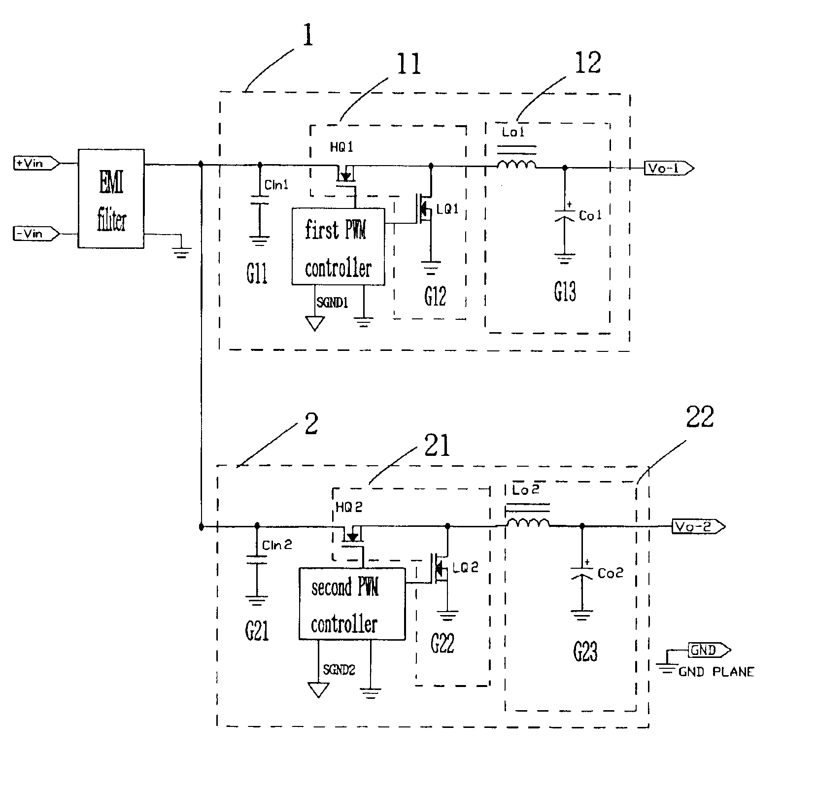
Please refer to FIG. 1 illustrating a circuit block diagram of a power supply...


PUM


Abstract

A method for eliminating noise interference and acoustic noise by a printed circuit board ground plane layout is disclosed. The method is applied to a circuit system having multiple outputs, wherein the circuit system has a first power converting module, a second power converting module and a printed circuit board. The first power converting module and the second power converting module respectively includes a first ground pin group and a second ground pin group. The method includes the steps of (a) connecting each ground pin of the first ground pin group to a respective solder point and connecting each solder point to a first node, and connecting each ground pin of the second ground pin group to a respective solder point and connecting each solder point to a second node, and (b) connecting the first node and the second node to a common node and connecting the common node to a solder point of a common ground terminal on the printed circuit board ground plane.

Description

FIELD OF THE INVENTIONThis invention relates to a method for eliminating noise interference and acoustic noise by a printed circuit board ground plane layout, and more particular to a method for eliminating noise interference and acoustic noise by a printed circuit board ground plane layout used in a power supply system having multiple outputs.BACKGROUND OF THE INVENTIONBecause of the progress of technologies, various electronic products have been shown up in the marketplace. It is widely known that the core of an electronic products is a printed circuit board. The normal operation of the electronic element mounted on a printed circuit board is a key factor for allowing an electronic product to function normally. However, signals of different frequencies are present in electronic circuits and systems. When there exists a frequency difference between signals, a mutual interference between electronic circuits and systems will be produced and cause the electronic product unstable or pr...

Claims


Application Information

Patent Timeline
Patent Type & Authority Patents(United States)
IPC IPC(8): H02M3/00H05K1/02
CPCH02M3/00H05K1/0216H05K2201/09663H05K2201/093H05K2201/09254H02M3/003
Inventor OUYANG, JR-HONGLAI, HUI-CHUANLIN, JING-CHENG
Owner DELTA ELECTRONICS INC
Learn More