
Semiconductor device having a matrix array of contacts and a fabrication process thereof

a technology of semiconductor devices and contacts, applied in the direction of individual semiconductor device testing, semiconductor/solid-state device testing/measurement, instruments, etc., can solve the problems of increasing the cost of lsi chip testing, the foregoing testing process, and the inability to test all solder balls, so as to reduce the number of testing boards needed for testing, reduce the cost of the semiconductor device, and reduce the time needed for writing test programs for each of the testing boards

Inactive Publication Date: 2005-01-18
SOCIONEXT INC
View PDF12 Cites 2 Cited by
  • Summary
  • Abstract
  • Description
  • Claims
  • Application Information

AI Technical Summary

Benefits of technology

Another and more specific object of the present invention is to provide a semiconductor device and a fabrication process thereof wherein the number of testing steps for testing the fabricated semiconductor device is reduced.
Another object of the present invention is to provide a semiconductor device and a fabrication process thereof wherein the number of testing boards used for testing the fabricated semiconductor device is reduced.
Another object of the present invention is to provide a semiconductor device and a fabrication process thereof wherein the number of testing programs used for testing the fabricated semiconductor device is reduced.
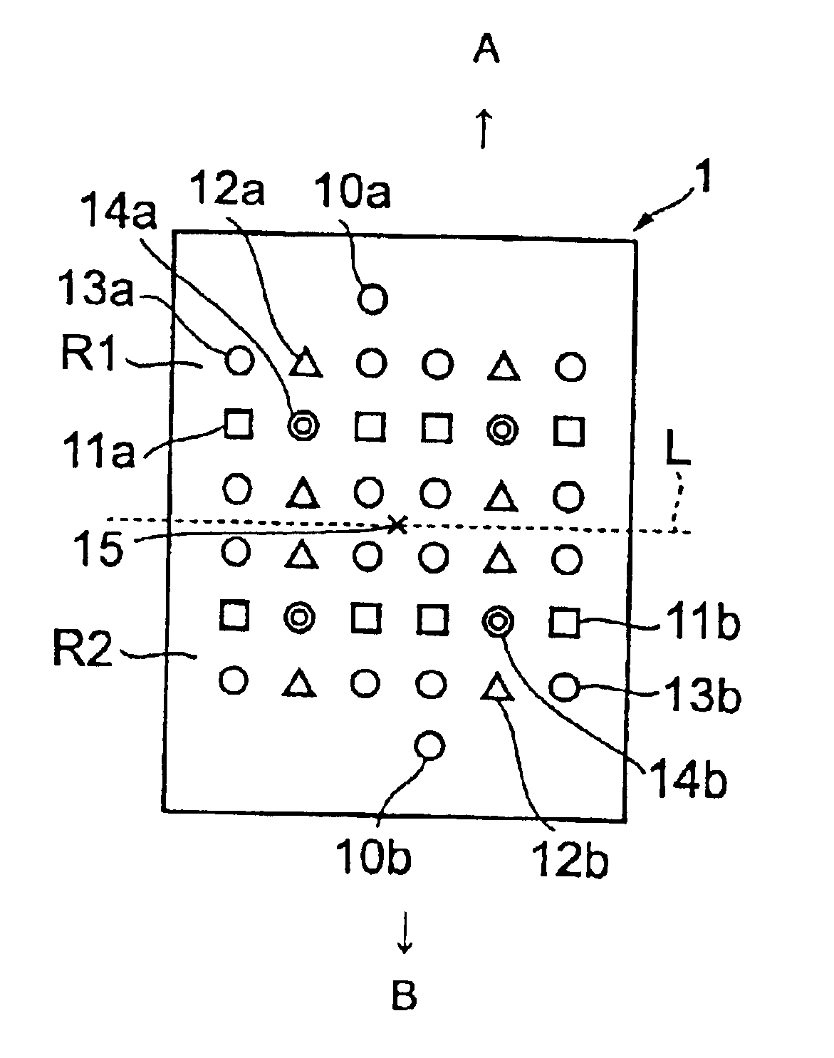
According to the present invention, it is possible to align the contact electrodes on the semiconductor chip, when the semiconductor device is mounted on a testing board carrying thereon contact pins in correspondence to the contact electrodes on the semiconductor chip, in any of first and second regions defined on the principal surface of the semiconductor chip, such that contact electrodes are aligned with the contact pins on the testing board according to the types of the signals; by merely rotating the semiconductor chip about the foregoing center of axial symmetry. Thereby, the number of the testing boards necessary for the testing is reduced and the cost of the semiconductor device is reduced. Further, the present invention uses only one testing program for the testing of the entire LSI chip and the time needed for writing test programs for each of the testing boards is reduced. In addition, the time needed for loading and unloading the testing programs is reduced.
Another object of the present invention is to provide a semiconductor device and a fabrication process thereof wherein the number of the testing boards used for testing the fabricated semiconductor device is reduced and the number of the testing programs used for testing the fabricated semiconductor device is reduced, while simultaneously guaranteeing a flexible designing of the semiconductor device.
According to the present invention, the correspondence between the terminals on the semiconductor device and the testing terminals on the testing board is maintained as a result of the use of the sockets, and the testing of the semiconductor device can be achieved while using the same testing board and the same testing program. By using the sockets in combination with the testing apparatus, the axial symmetry for the arrangement of the terminals is no longer required in the semiconductor device, and the degree of freedom for designing the semiconductor device is increased.

Problems solved by technology

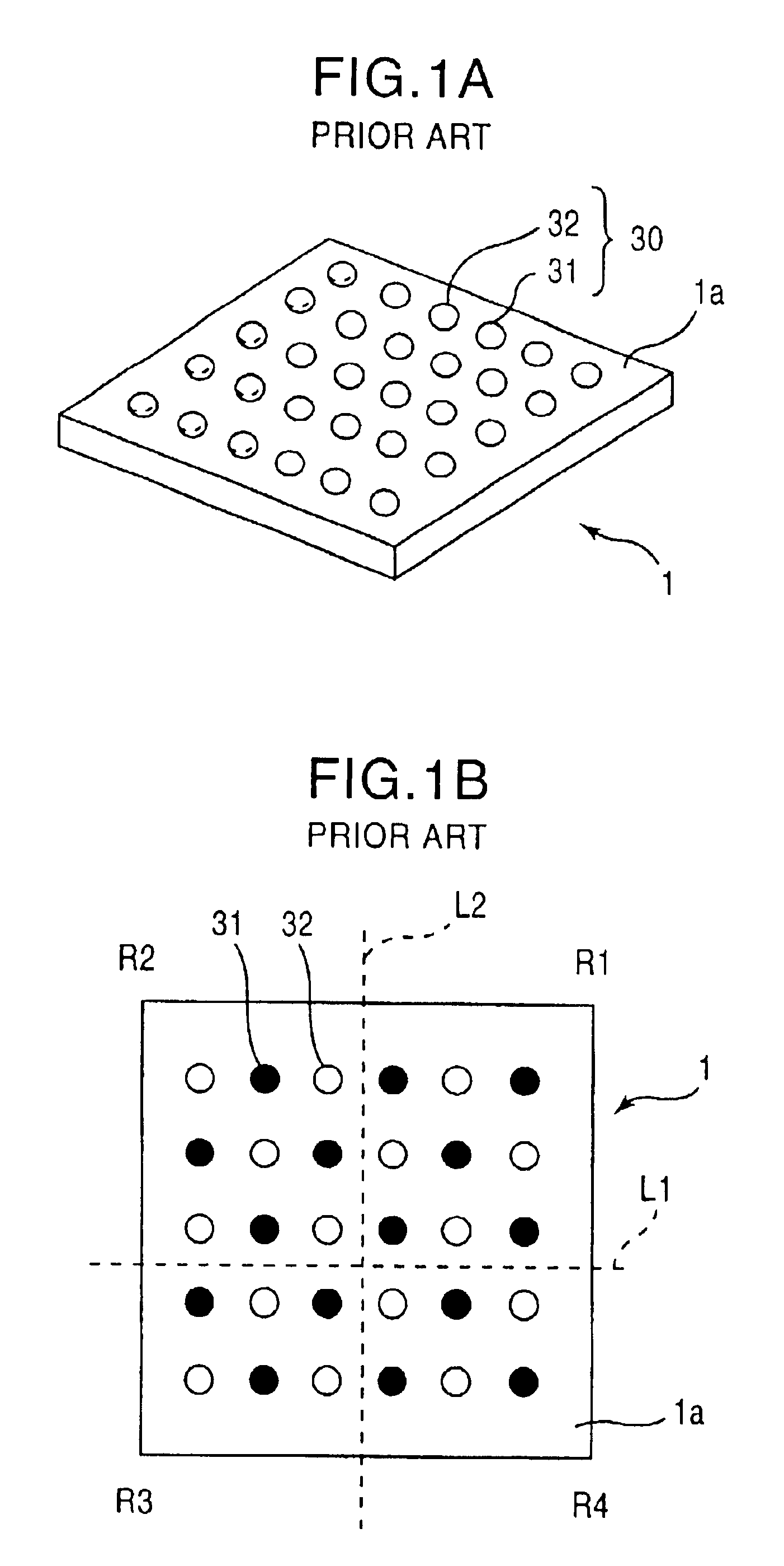
In the case of recent LSI chips carrying a very large number of solder balls 30 on the chip principal surface 1a, it should be noted that the number of the solder balls 30 can exceed the number of the test terminals provided on the testing board, and there arises a problem in that the testing is not possible for all of the solder balls 30 on the chip 1.
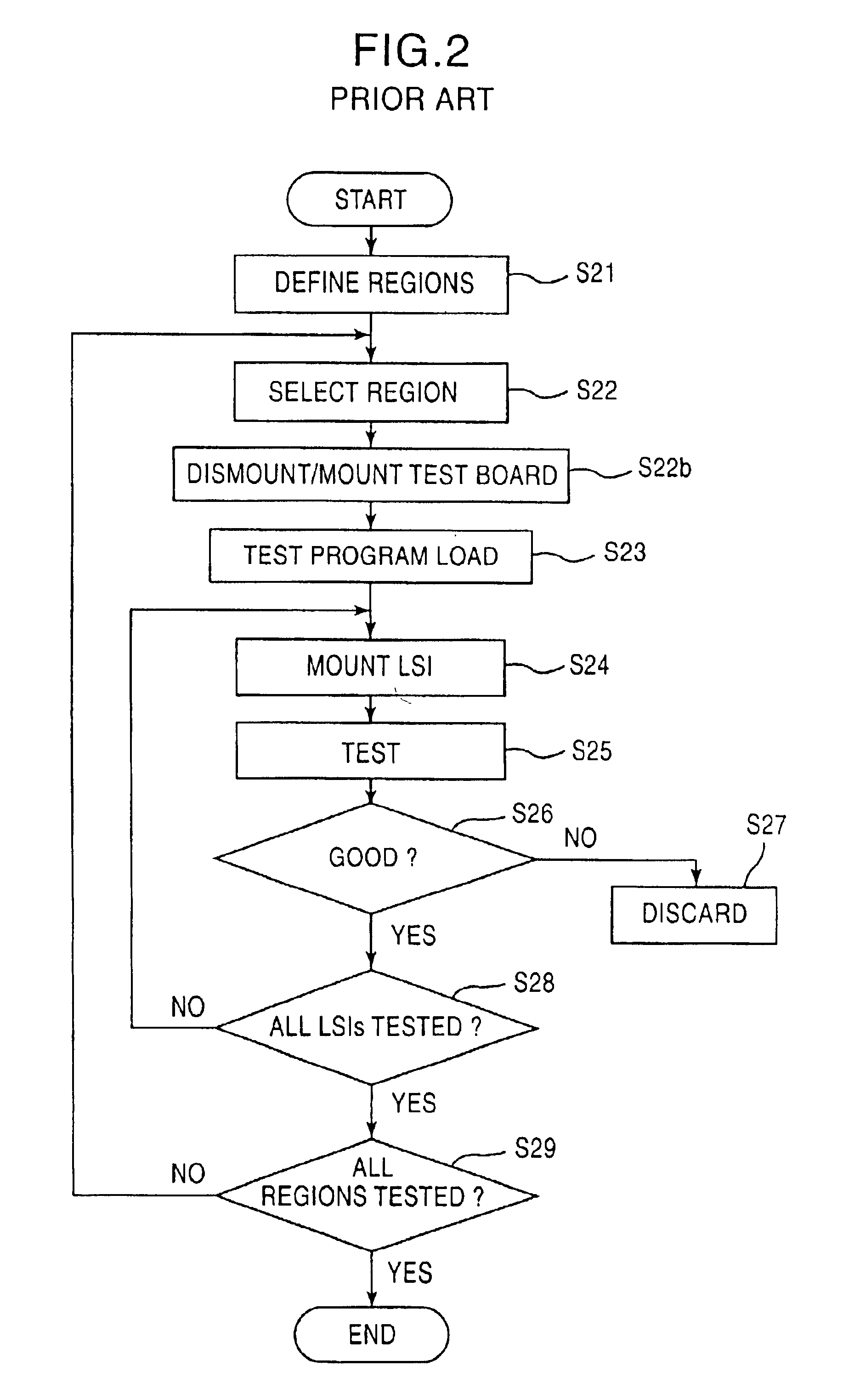
However, the foregoing testing process has a drawback in that it is necessary to provide a number of testing boards 2a and 2b in correspondence to arbitrarily defined regions R1-R4.
Thereby, the cost of the testing of the LSI chip increases inevitably.
Further, the foregoing testing process has a drawback in that it requires a large number of testing steps including loading and unloading of the testing programs, mounting and dismounting of the LSI chips, and the like.

Method used


Image

  • Semiconductor device having a matrix array of contacts and a fabrication process thereof
  • Semiconductor device having a matrix array of contacts and a fabrication process thereof
  • Semiconductor device having a matrix array of contacts and a fabrication process thereof

Examples


first embodiment

[First Embodiment]

FIG. 4 shows the construction of an LSI chip 1 according to a first embodiment of the present invention in a bottom view.

Referring to FIG. 4, the LSI chip 1 carries, on a bottom surface thereof, various contact electrodes including TAP (test access port) terminals 10a and 10b, power supply terminals (VDD) 11, ground terminals (GND) 12, signal input terminals 13 and signal output terminals 14, wherein it should be noted that the bottom surface of the LSI chip 1 is divided into a first region R1 and a second region R2 by a boundary line L. Thereby, the foregoing terminals are also divided into two groups such that the terminals in the first region R1 are symmetrical with the corresponding terminals in the second region R2 about a form center 15 of the LSI chip 1. In other words, there is a diad axis in correspondence to the form center 15.

For example, the TAP terminal 10a in the region R1 is formed such that the terminal 10a coincides with the corresponding TAP termi...

second embodiment

[Second Embodiment]

FIG. 9 shows the bottom view of the LSI chip 1 according to a second embodiment of the present invention, wherein those parts corresponding to the parts described previously are designated by the same reference numerals and the description thereof will be omitted.

Referring to FIG. 9, the LSI chip 1 of the present invention has a bottom surface divided into regions RA-RD by the boundary lines L1 and L2, wherein the region RA includes a test control terminal 9a, a power (VDD) terminal 11a, a power (GND) terminal 12a, a signal input terminal 13a and a signal output terminal 14a.

Similarly to the first embodiment, the foregoing terminals are arranged symmetric with respect to the form center 15 such that the each terminal comes to the overlapping location of a terminal of the same kind after rotation about the foregoing form center 15 by an angle of 90°. In other words, there appears a 90-degree axial symmetry in the bottom surface of the LSI chip 1.

FIG. 10 shows the ...

third embodiment

[Third Embodiment]

In the foregoing first and second embodiments, there arises problems noted below.

The first problem arises in relation to the mode of mounting of the LSI chip 1 on the testing board 2, in that the LSI chip 1 is mounted on the testing board 2 in the progressively rotated state. In view of the fact that the same testing program is used throughout in the foregoing embodiments, there arises a difficulty in relating the result of the testing and the region of the LSI chip 1 that has been tested. Further, there arises a difficulty to recognize whether or not the entire regions of the LSI chip 1 have been tested.

The second problem is that, due to the requirement of axial symmetry in the arrangement of the terminals, the degree of freedom in designing the LSI chip is reduced substantially.

FIG. 11 shows the bottom view of the LSI chip 1 according to a third embodiment of the present invention in which the foregoing first problem is addressed, wherein those parts of FIG. 11 c...


PUM


Abstract

A semiconductor device includes a semiconductor chip carrying a plurality of contact electrodes on a principal surface thereof, wherein the contact electrodes are arranged symmetrically about an axis of symmetry according to the types of the contact electrodes.

Description

BACKGROUND OF THE INVENTIONThe present invention generally relates to semiconductor devices and more particularly to a fabrication process of a semiconductor device having a matrix array of contacts including a pin grid array or a ball grid array and a fabrication process thereof.With the advancement in the art of device miniaturization, recent highly integrated LSI chips generally carry a very large number of contact electrodes thereon for external interconnection. For example, there are LSI chips that carry the contact electrodes with a number of several hundreds or even one thousand.FIG. 1A shows an example of such an LSI chip 1 of the so-called BGA (ball grid array) type in which a number of solder balls 30 are provided on a principal surface 1a thereof in a row and column formation as the contact electrodes. There are LSI chips of this type in which the number of the solder balls 30 exceeds 500. The solder balls 30 on the chip 1 includes power supply terminals 31 and input / outp...

Claims


Application Information

Patent Timeline
Patent Type & Authority Patents(United States)
IPC IPC(8): H01L23/50H01L23/48
CPCH01L23/50H01L2924/3011H01L2924/0002H01L2924/00H01L2224/0615H01L2224/06154H01L2224/06151
Inventor YAMADA, NAOTOKOBAYASHI, NORIHIRO
Owner SOCIONEXT INC
Learn More