
Processing method and processing apparatus

a processing apparatus and processing method technology, applied in the field of processing methods and processing apparatuses, can solve the problems of large size of entire units, and increased facility costs of units,

Inactive Publication Date: 2004-10-05
TOKYO ELECTRON LTD
View PDF5 Cites 9 Cited by
  • Summary
  • Abstract
  • Description
  • Claims
  • Application Information

AI Technical Summary

Benefits of technology

The present invention relates to a processing method and apparatus for successively processing multiple workpieces in different process conditions while keeping the size reduction of the apparatus. The technical effect of the invention is to allow for the processing of multiple workpieces in different types of process conditions while keeping the size reduction of the apparatus. This is achieved by setting different process portions for processing the workpieces and changing the process conditions accordingly. The invention also includes a method for repeatedly processing the workpieces in different process conditions while keeping the size reduction of the apparatus. This allows for the processing of multiple workpieces in different types of process conditions without the need for additional thermal process units or long cool-down periods, which can decrease process performance and increase facility costs.

Problems solved by technology

However, when two sets of thermal process units are prepared, the size of the entire units might become large.
In addition, the facility cost of the units might rise.
In particular, when LCD substrates that are becoming large year by year, which is a current tendency, are produced, the entire units become very large.
In contrast, in the case that the temperatures of one thermal process unit are changed, although the size of the unit can be reduced, it might take a long time until a desired process temperature has been set.

Method used


Image

  • Processing method and processing apparatus
  • Processing method and processing apparatus
  • Processing method and processing apparatus

Examples


Embodiment Construction

Next, with reference to the accompanying drawings, embodiments of the present invention will be described in detail.

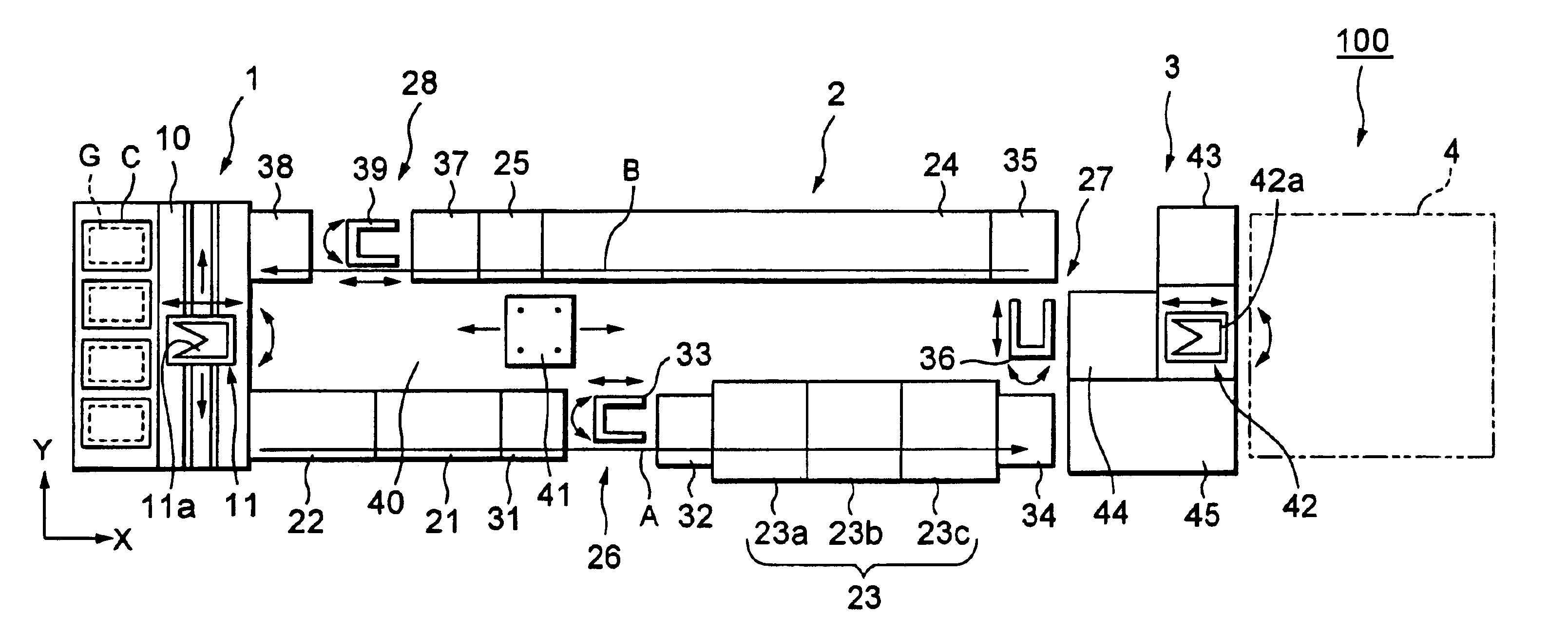
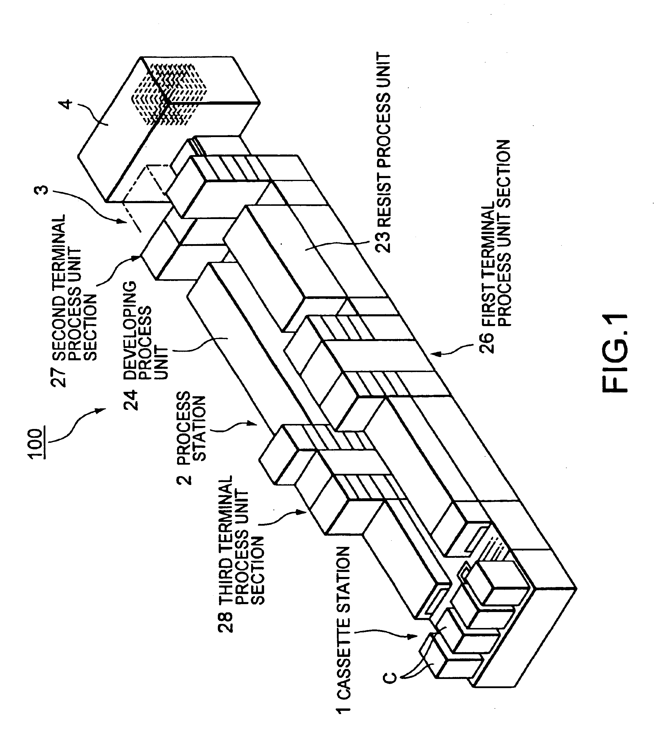
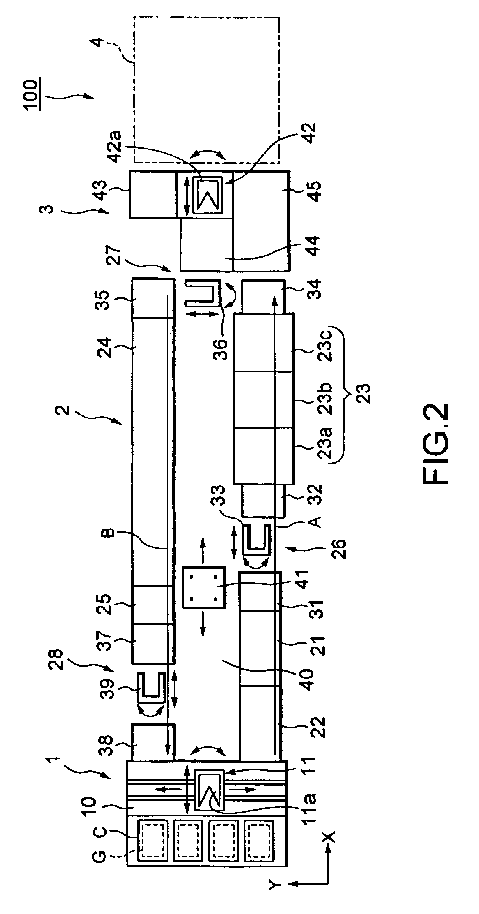
FIG. 1 is a perspective view showing a resist coating and developing process system for LCD glass substrates, the system having a processing apparatus according to the present invention. FIG. 2 is a plan view showing an outline of the resist coating and developing process system.

The resist coating and developing process system 100 has a cassette station 1 (loading and unloading portion), a process station 2 (process portion), and an interface station 3 (interface portion). On the cassette station 1, cassettes C are placed. Each cassette C contains a plurality of LCD glass substrates (hereinafter referred to as substrates G) as workpieces. The process station 2 has a plurality of process units that perform a sequence of processes including a resist coating process and a developing process. The interface station 3 transfers substrates G with an exposing unit 4. The casse...


PUM

PropertyMeasurementUnit
heightaaaaaaaaaa
temperatureaaaaaaaaaa

Abstract

After the first workpieces have been processed in the first process portion while the second workpieces are being processed in the second process portion, the first process portion in which the first process condition has been set for the third process condition. By repeating such processes, a plurality of workpieces can be successively processed in different types of process conditions.

Description

1. Field of the InventionThe present invention relates to a processing method and a processing apparatus, in particular, a processing method and a processing apparatus for successively processing a plurality of workpieces such as glass substrates for liquid crystal display devices (LCD), semiconductor wafers, and so forth in different process conditions.2. Description of the Related ArtGenerally, when an LCD is produced, like in a semiconductor wafer producing process, a predetermined film is formed on an LCD glass substrate (hereinafter referred to as LCD substrate) as a workpiece. Thereafter, a photoresist solution is coated on the formed film. As a result, a resist film is formed. The resist film is exposed corresponding to a predetermined circuit pattern. Thereafter, a developing process is performed for the resist film. In such a manner, namely by so-called photolithography technology, the circuit pattern is formed.In the photolithography technology, after a cleaning process is...

Claims


Application Information

Patent Timeline
Patent Type & Authority Patents(United States)
IPC IPC(8): G03D3/00H01L21/027
CPCG03D3/00A47B13/083A47B13/16A47B17/06A47B95/00A47B2220/0075A47D3/00A47D15/00C09D1/00H04R1/028H04R2430/01
Inventor TATEYAMA, KIYOHISA
Owner TOKYO ELECTRON LTD
Learn More