Dielectric composites
a technology of dielectric composites and dielectric medium, which is applied in the direction of additive manufacturing processes, cameras, instruments, etc., can solve the problem of proven impracticality of fabricating using drilling methods
- Summary
- Abstract
- Description
- Claims
- Application Information
AI Technical Summary
Problems solved by technology
Method used
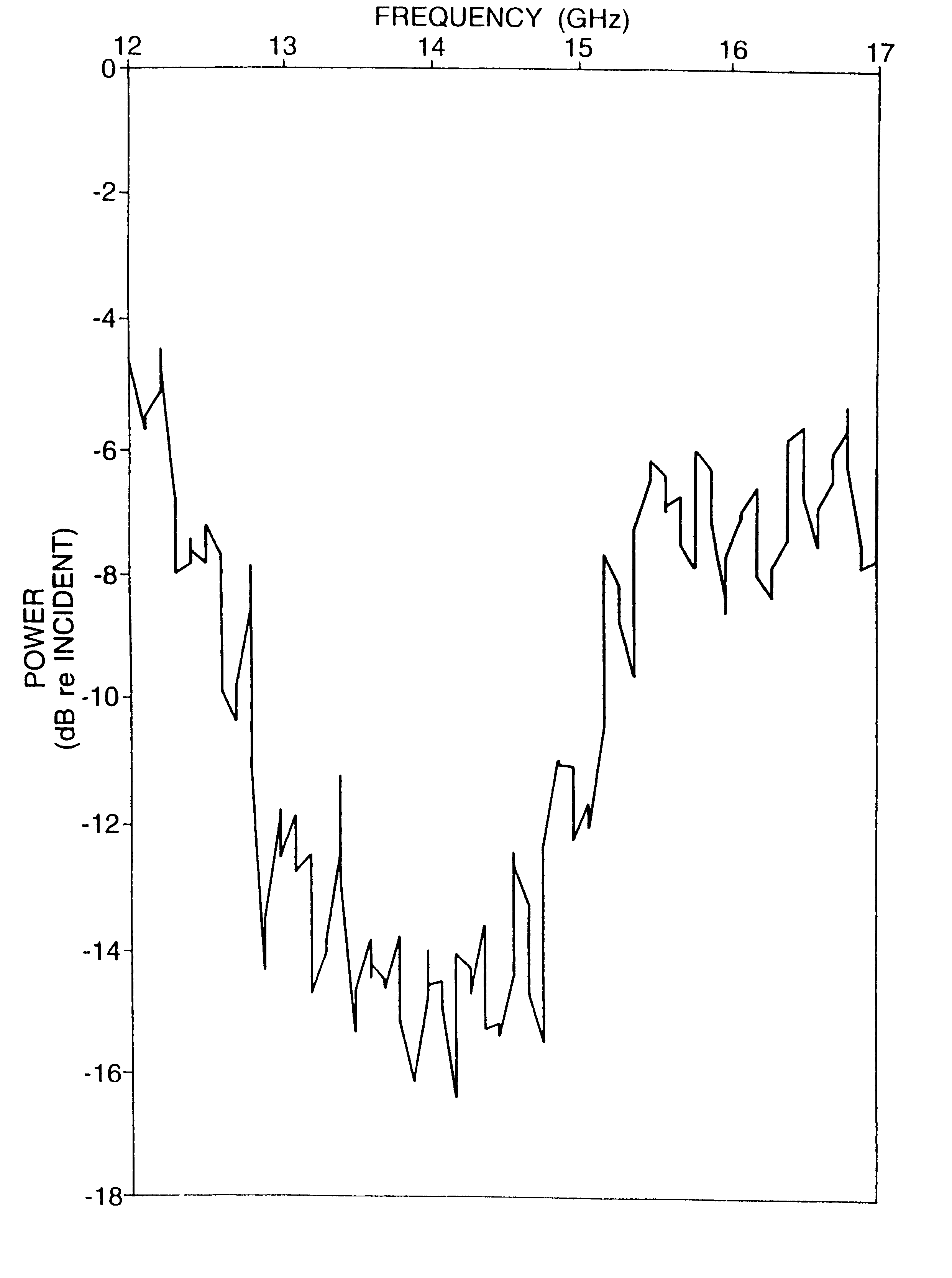
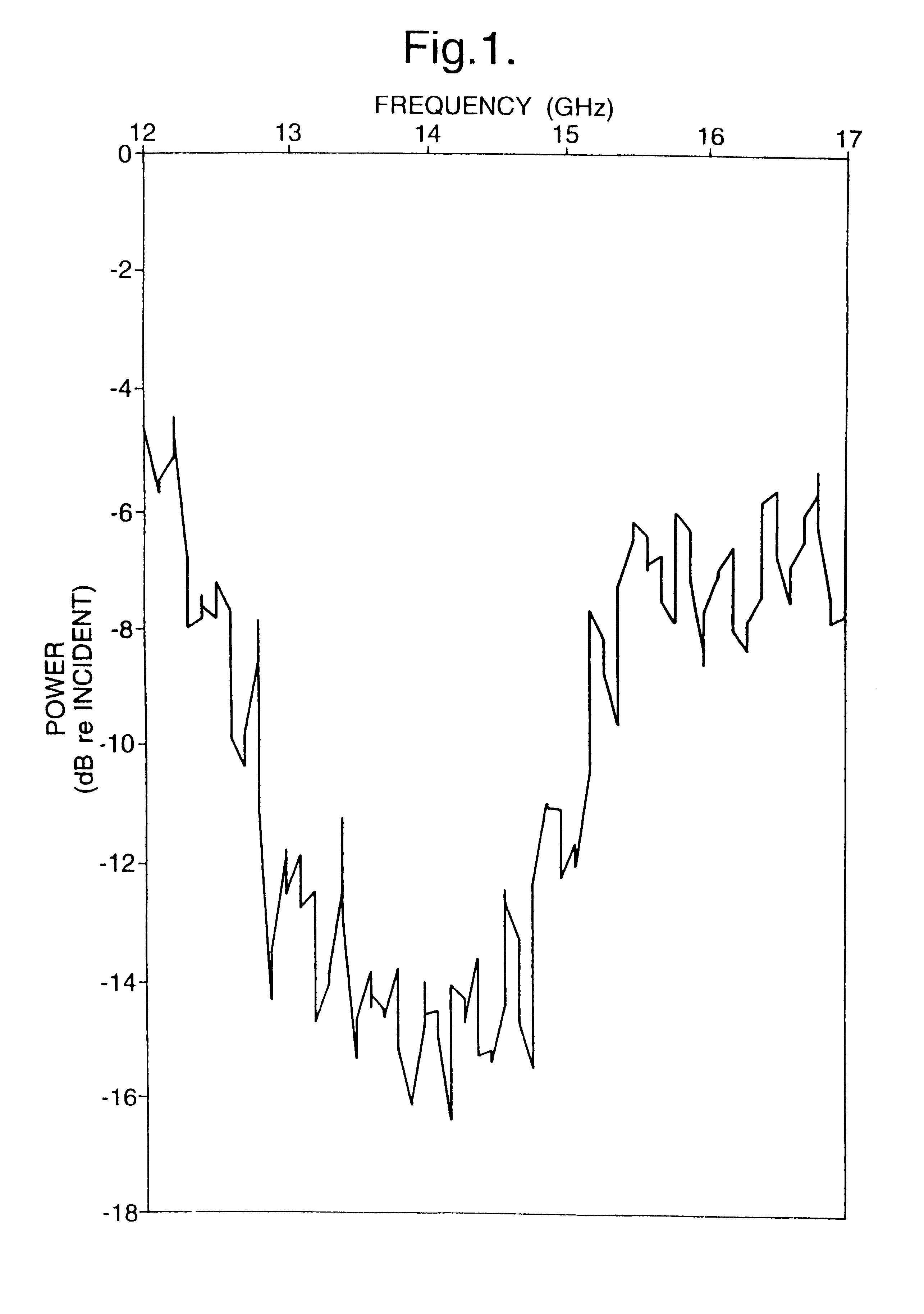
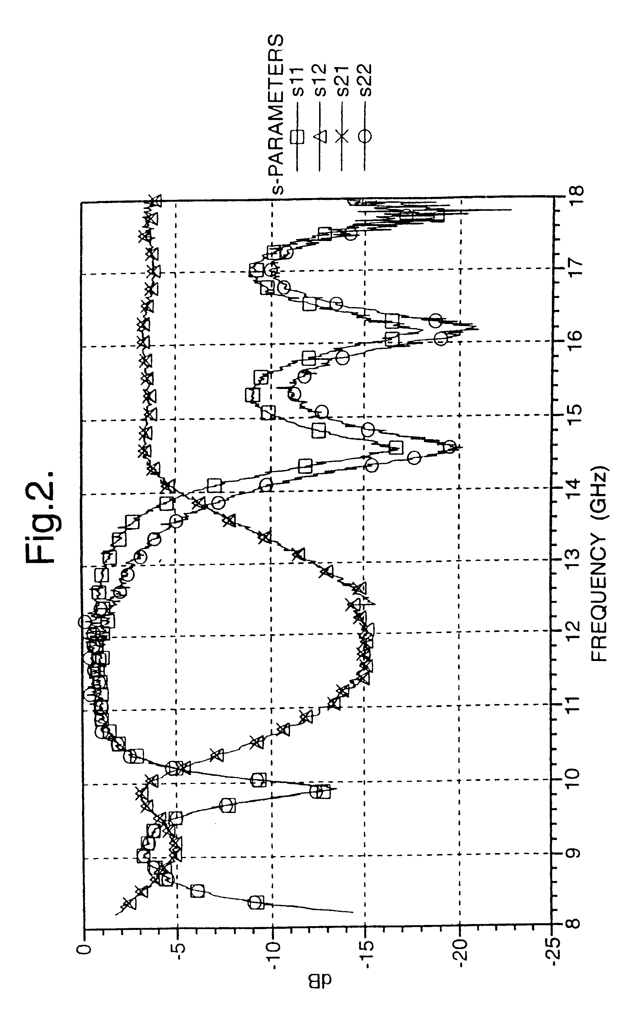
Image

Examples
Embodiment Construction
The main manufacturer of SLA machines is 3D Systems of Valencia, Calif., USA. The SLA-250 / 40 machine used in the specific embodiment of this invention consists of an ultra-violet-(UV)-screened cabinet containing a 254 mm.times.254 mm.times.254 mm vat of SL-5170 liquid resin. The resin, manufactured by Ciba-Geigy (CIBATOOL.RTM. SL resin), is curable by exposure to ultraviolet light. The system includes a 25 mW HeCd laser, emitting at 325 mm.
An internal optical system directs the laser beam onto the surface of the resin, where the beam width is approximately 0.2 mm. The optical system scans the beam across the surface of the resin according to digital instructions relayed from an attached PC computer.
Local curing takes place at the surface of the resin. A complete scan of the surface selectively polymerises a layer of resin of thickness 0.125 mm on an elevator platform positioned just below the surface. After each layer scan the elevator platform is lowered into the resin vat and then...
PUM
| Property | Measurement | Unit |
|---|---|---|
| Dielectric polarization enthalpy | aaaaa | aaaaa |
| Permittivity | aaaaa | aaaaa |
Abstract
Description
Claims
Application Information
 - R&D Engineer
- R&D Manager
- IP Professional
- Industry Leading Data Capabilities
- Powerful AI technology
- Patent DNA Extraction
Browse by: Latest US Patents, China's latest patents, Technical Efficacy Thesaurus, Application Domain, Technology Topic.
© 2024 PatSnap. All rights reserved.Legal|Privacy policy|Modern Slavery Act Transparency Statement|Sitemap