
Programmable impedance control circuit

a control circuit and impedance technology, applied in logic circuit coupling/interface arrangement, pulse technique, instruments, etc., can solve the problems of mismatch errors in the measurement of external impedance by the controller, increase the consumption of power, and difficulty in properly terminating with matching impedance with fixed resistan

Inactive Publication Date: 2003-02-25
SAMSUNG ELECTRONICS CO LTD
View PDF2 Cites 97 Cited by
  • Summary
  • Abstract
  • Description
  • Claims
  • Application Information

AI Technical Summary

Problems solved by technology

Parallel terminations exhibit superior signal integrity than series terminations, but consume more power.
However, because the output driver and the on-chip termination are disposed within a chip and characteristic impedance varies depending upon operating conditions, it is difficult to properly terminate with matching impedance with a fixed resistance.
Another problem is that there may be mismatch errors in the measurement of the external impedance by the controller, because at high frequencies the external resistance may differ from the external impedance.
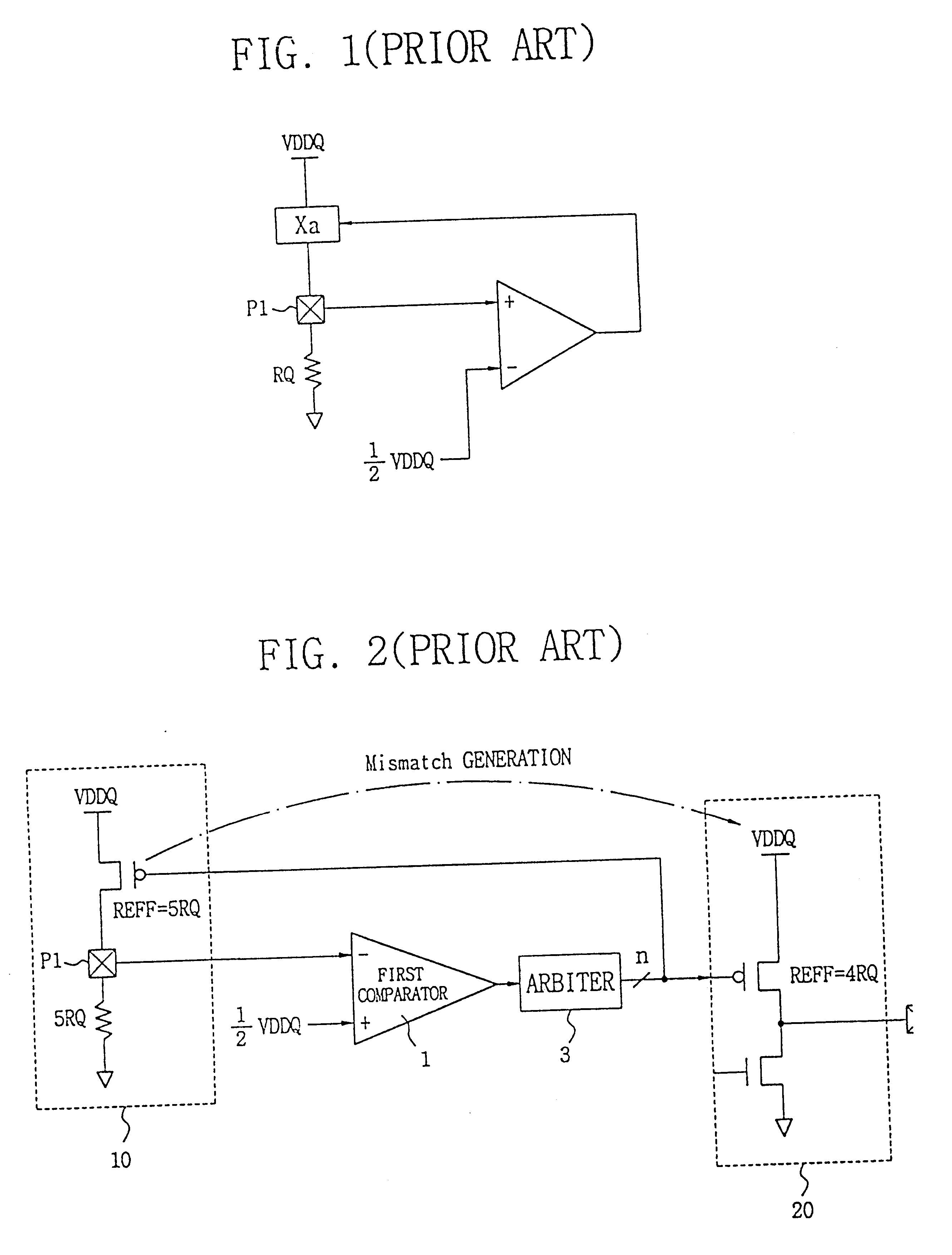
This is done by providing a second set of transistors 20 that has a 5 / 4 ratio as compared to the size of the first transistor 10, but there is a possibility that mismatching can result from the difference in transistor size.
In addition, because the circuit generates only one extra termination impedance, the circuit could not provide portions such as output buffer DQ, control, address, and clock pin, etc., which need various impedances.

Method used


Image

  • Programmable impedance control circuit
  • Programmable impedance control circuit
  • Programmable impedance control circuit

Examples


first embodiment

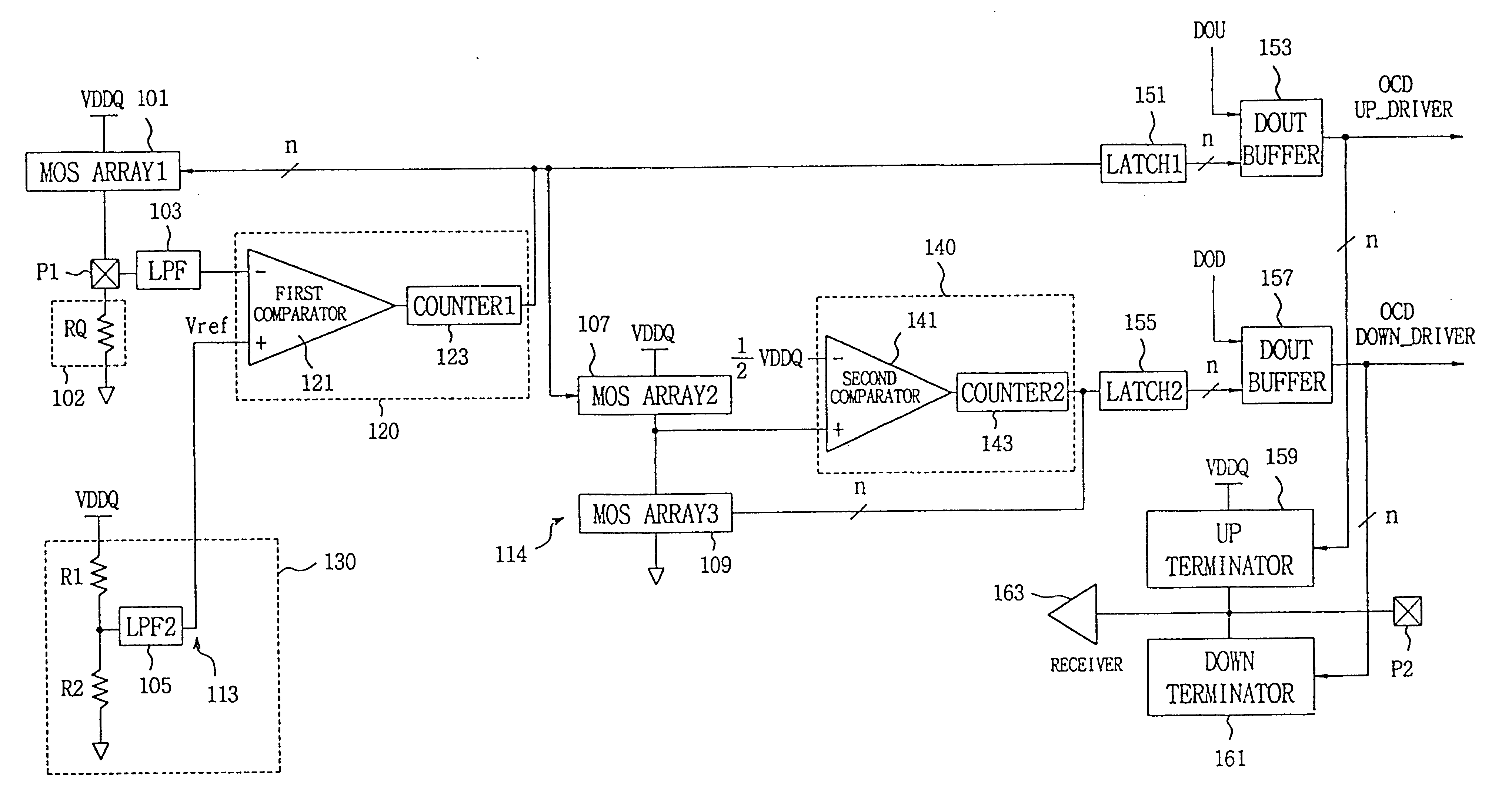
Referring to FIG. 7, there is shown a schematic of a programmable impedance control circuit in which an optional reference voltage is employed according to the present invention. The circuit comprises a pull-up circuit comprising a first MOS array 101 connected to VDDQ, a first pad P1, an external resistance 102 RQ, a low-pass filter LPF 103, a reference voltage generator 130, a first detector 120, a first latch 151, a first data output buffer 153, an off-chip up-driver OCD UP_DRIVER, and an up-terminator 159.

Also provided is a pull-down circuit comprising a second MOS array 107, a third MOS array 109, a second detector 140, a second latch 155, a second data output buffer 157, an off-chip down-driver OCD DOWN-DRIVER and a down-terminator 161.

The circuit uses M times internal impedance (N.noteq.M) in accordance with N times the external impedance RQ attached to the system by the user. Its operation is as follows:

First, the first MOS array 101 in the pull-up circuit is supplied with t...

second embodiment

Next, the operation of the programmable impedance control circuit for generating an optional reference voltage by an analog method according to the present invention is explained in detail with reference to FIG. 8.

FIG. 8 is a schematic of another embodiment of the invention. In this circuit, when a current source is used as a detecting circuit and a reference voltage is adopted as (5 / 8)VDDQ, the flowing current is the same as when the VDDQ / 2 voltage is connected to a .times.4 external resistance. A current source PMOS1 is supplied with VDDQ or VDD voltage. The circuit does not become responsive to noises in the pad P1 because of the PMOS1. The external resistance RQ has an N times the external impedance. The pad P1 outputs the voltage obtained in combination of the PMOS1 and the external resistance RQ. The first reference voltage generator 210 generates the reference voltage corresponding to N / (N+M) times VDDQ. The first comparator 223 compares the output voltage from the pad P1 wit...


PUM


Abstract

Disclosed is a programmable impedance control circuit, comprising a voltage divider, the voltage divider comprising an MOS array supplied with a first voltage and an external resistance having an external impedance equal to N times said external resistance. The voltage divider outputs a second voltage. A reference voltage generator is provided for generating a third voltage corresponding to N / (N+M) times said first voltage as a reference voltage for said second voltage, and wherein M times internal impedance is used for N times external impedance (N=M or N<> M).

Description

1. Field of the InventionThe present invention relates to a programmable impedance control circuit and more particularly to a programmable impedance control circuit that produces an internal impedance related to an external impedance.2. Description of the Related ArtRecently, methods of combining on-chip parallel termination with series termination have been proposed for high speed data transmission (HSDT) applications. Parallel terminations exhibit superior signal integrity than series terminations, but consume more power. In on-chip terminated HSDT applications, full swing data is typically transmitted through a transmission line wherein an output driver acts as a source termination and a receiver acts as a parallel termination. In such a method, the swing level of the signal may be lowered. To implement on-chip termination, a matching resistor should be added to the output driver. However, because the output driver and the on-chip termination are disposed within a chip and charac...

Claims


Application Information

Patent Timeline
Patent Type & Authority Patents(United States)
IPC IPC(8): H03H21/00H03H11/40H03H11/02H01L27/04G11C11/00H01L21/822H03H7/38H03H11/28H03K19/0175
CPCH03H21/0001H03H11/405G11C11/00
Inventor KIM, NAM-SEOGCHO, UK-RAE
Owner SAMSUNG ELECTRONICS CO LTD
Learn More