Frequency variable filter, antenna duplexer, and communication apparatus incorporating the same
a technology of frequency variable filter and duplexer, which is applied in the direction of resonators, electrical devices, waveguides, etc., can solve the problem of limited design freedom of conventional filters
- Summary
- Abstract
- Description
- Claims
- Application Information
AI Technical Summary
Benefits of technology
Problems solved by technology
Method used
Image
Examples
first embodiment
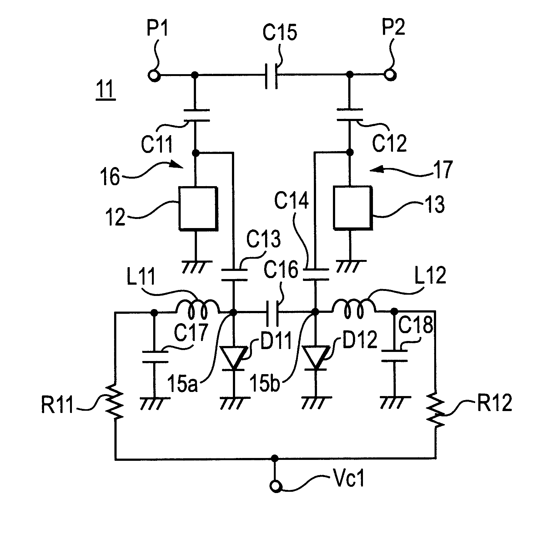
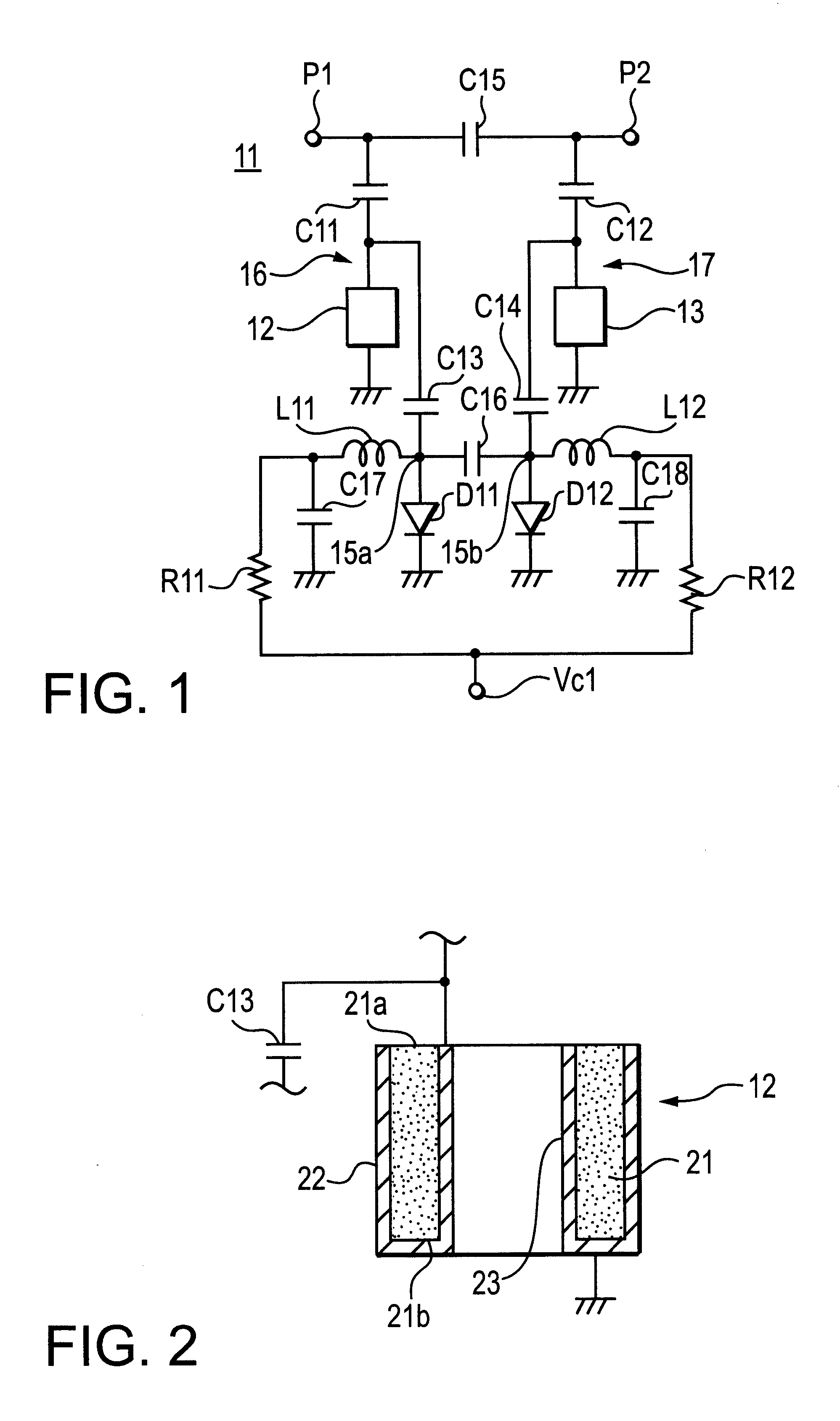
As shown in FIG. 1, in a frequency variable band elimination filter 11, between an input external terminal P1 and an output external terminal P2, a trap circuit having a serial resonance section 16 composed of a resonator 12 and a resonance capacitor C11 is electrically connected to a trap circuit having a serial resonance section 17 composed of a resonator 13 and a resonance capacitor C12 via a capacitor C15. The resonance capacitors C11 and C12 are capacitors for determining the amount of elimination-band attenuation. Instead of the capacitor C15, a coupling coil or a parallel circuit composed of a coupling coil and a coupling capacitor may be used.
A serial circuit composed of a frequency shifting capacitor C13 and a PIN diode D11 as a voltage-controllable reactance element is electrically connected to the open-circuited-end of the resonator 12 in parallel to the resonator 12 and the cathode of the PIN diode D11 is grounded. Similarly, a serial circuit composed of a frequency shif...
second embodiment
As a second embodiment of the invention, there is shown an antenna duplexer. As shown in FIG. 7, in an antenna duplexer 141, a transmission filter 142 is electrically connected between a transmission terminal Tx and an antenna terminal ANT, and a reception filter 143 is electrically connected between a reception terminal Rx and the antenna terminal ANT. In this case, the dielectric filter 11 of the first embodiment can be used as each of the transmission filter 142 and the reception filter 143. By use of the dielectric filter 11, the antenna duplexer 141 has greater freedom of design and can be made compact.
third embodiment
As a third embodiment of the present invention, there is shown a communication apparatus. A mobile phone will be illustrated as an example for the third embodiment.
FIG. 8 is an electric circuit block diagram of the RF section of a mobile phone 150. In FIG. 8, the reference numeral 152 denotes an antenna element, the reference numeral 153 denotes a duplexer, the reference numeral 161 denotes a transmission-side isolator, the reference numeral 162 denotes a transmission-side amplifier, the reference numeral 163 denotes a transmission-side interstage band pass filter, the reference numeral 164 denotes a transmission-side mixer, the reference numeral 165 denotes a reception-side amplifier, the reference numeral 166 denotes a reception-side interstage band pass filter, the reference numeral 167 denotes a reception-side mixer, the reference numeral 168 denotes a voltage-controlled oscillator (VCO), and the reference numeral 169 denotes a local band pass filter.
In this case, as the duplexe...
PUM
 Abstract
Description
Claims
Application Information
 - R&D
- Intellectual Property
- Life Sciences
- Materials
- Tech Scout
- Unparalleled Data Quality
- Higher Quality Content
- 60% Fewer Hallucinations
Browse by: Latest US Patents, China's latest patents, Technical Efficacy Thesaurus, Application Domain, Technology Topic, Popular Technical Reports.
© 2025 PatSnap. All rights reserved.Legal|Privacy policy|Modern Slavery Act Transparency Statement|Sitemap|About US| Contact US: help@patsnap.com


