Optical information recording medium, manufacturing method therefor, manufacturing apparatus therefor, and optical information recording and reproducing apparatus
a manufacturing method and optical information technology, applied in the direction of digital signal error detection/correction, head carrier alignment, disposition/mounting of heads, etc., can solve the problems of manufacturing yield unsatisfactory, manufacturing optical disks can be deformed, and only a single information layer structure for recording information encounters limitations
- Summary
- Abstract
- Description
- Claims
- Application Information
AI Technical Summary
Benefits of technology
Problems solved by technology
Method used
Image
Examples
example 2
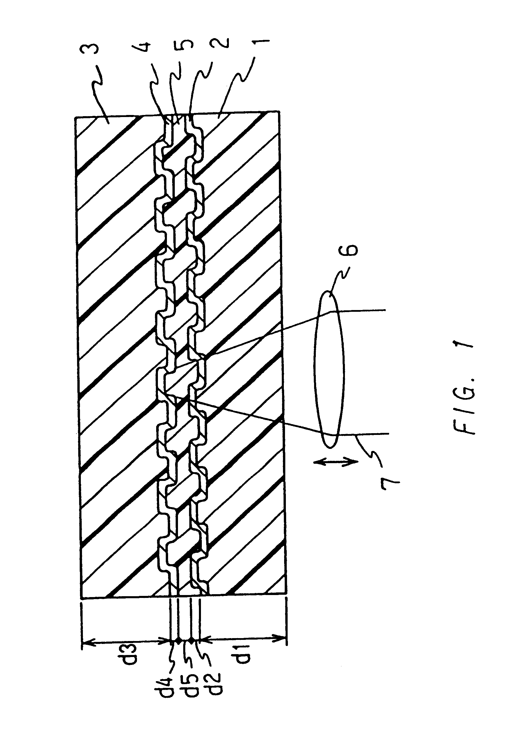
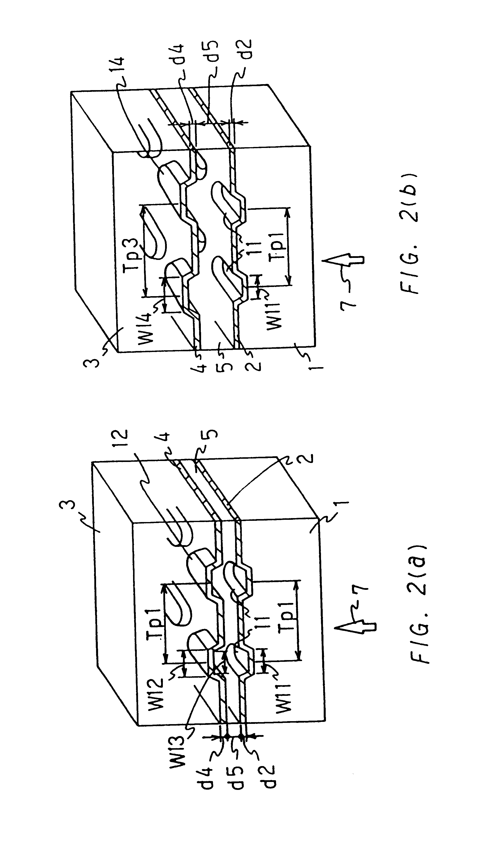
A structure of a recording medium capable of forming information more densely will now be described. Similarly to Example 1, polycarbonate resin was employed to form the first and second substrates 1 and 3, and a mold having a surface comprising information pits was used to perform injection molding so that the first and second substrates 1 and 3 were manufactured. The first substrate 1 had a thickness of 0.58 mm and comprised, on the surface thereof, information pits arranged such that the shortest pit length was 0.5 .mu.m, the pit depth was 90 nm and the track pitch was 0.8 .mu.m. On the first substrate 1, there was formed an Au layer having a thickness of 11 nm by a sputtering method so that the first information layer 2 was formed.
The second substrate 3 had the same thickness as that of the first substrate 1, the second substrate 3 having information pits in the same form as those of the first substrate 1. To make the directions of the spirals of the first substrate 1 and the se...
example 3
An example of a recording medium having four information layers as shown in FIG. 5 will now be described. Similarly to Example 1, polycarbonate resin was employed to form the first to fourth substrates 58, 60, 63 and 65, and a mold having a surface comprising information pits was used to perform injection molding so that the first to fourth substrates 58, 60, 63 and 65 were manufactured. Each of the first and third substrates had a thickness of 0.58 mm and comprised, on the surface thereof, information pits arranged such that the shortest pit length was 0.5 .mu.m, the pit depth was 90 nm and the track pitch was 0.8 .mu.m. On each of the first and third substrates 58 and 63, there was formed an Au layer having a thickness of 11 nm by a sputtering method so that the first and third information layers 59 and 64 were formed.
Each of the second and fourth substrates 60 and 65 had a thickness of 0.4 mm, which was smaller than that of each of the first and third substrates 58 and 63, in ord...
example 4
The specific structure of the optical information recording medium shown in FIG. 18 and recording and reproducing operations with the foregoing medium will now be described.
The first substrate 31 was made of polycarbonate resin and having, on the surface thereof, information pits formed in accordance with EFM modulation to correspond to information signals. The thickness d1 of the first substrate 31 was 0.58 mm and the diameter was 120 mm. The information pits formed on the surface of the first substrate 31 were arranged in such a manner that the shortest length of the pit of the pits formed on its surface was 0.44 .mu.m, the pitch depth was 90 nm and the track pitch was 0.74 .mu.m. A ZnS layer having a thickness of 40 nm was formed on the surface of the first substrate 31 by the sputtering method so that the first information layer 32 was formed.
The second substrate 33 was made of polycarbonate resin and had guide grooves for tracking light beams on the surface thereof. The second ...
PUM
| Property | Measurement | Unit |
|---|---|---|
| reflectance | aaaaa | aaaaa |
| relative humidity | aaaaa | aaaaa |
| temperature | aaaaa | aaaaa |
Abstract
Description
Claims
Application Information
 - R&D
- Intellectual Property
- Life Sciences
- Materials
- Tech Scout
- Unparalleled Data Quality
- Higher Quality Content
- 60% Fewer Hallucinations
Browse by: Latest US Patents, China's latest patents, Technical Efficacy Thesaurus, Application Domain, Technology Topic, Popular Technical Reports.
© 2025 PatSnap. All rights reserved.Legal|Privacy policy|Modern Slavery Act Transparency Statement|Sitemap|About US| Contact US: help@patsnap.com


