Method for producing a semiconductor device with an accurately controlled impurity concentration profile in the extension regions
a technology of impurity concentration and extension region, which is applied in the direction of semiconductor devices, electrical appliances, transistors, etc., can solve the problems of increasing speed of semiconductor devices, reducing power consumption of semiconductor devices, and achieving the effect of highly accurate control
- Summary
- Abstract
- Description
- Claims
- Application Information
AI Technical Summary
Benefits of technology
Problems solved by technology
Method used
Image

Examples
example 2
Example 2 is a variant of Example 1. In Example 2, between [Step-130] and [Step-140], gate-side-walls 30 are formed on the side walls of the gate electrode 21 such that at least the extension regions 25 are covered, and then, the surfaces of the source / drain regions 23 are converted to silicide surfaces. Mainly with regard to differences from Example 1, the method for producing a semiconductor device in Example 2 will be explained with reference to FIG. 4.
[Step-200]
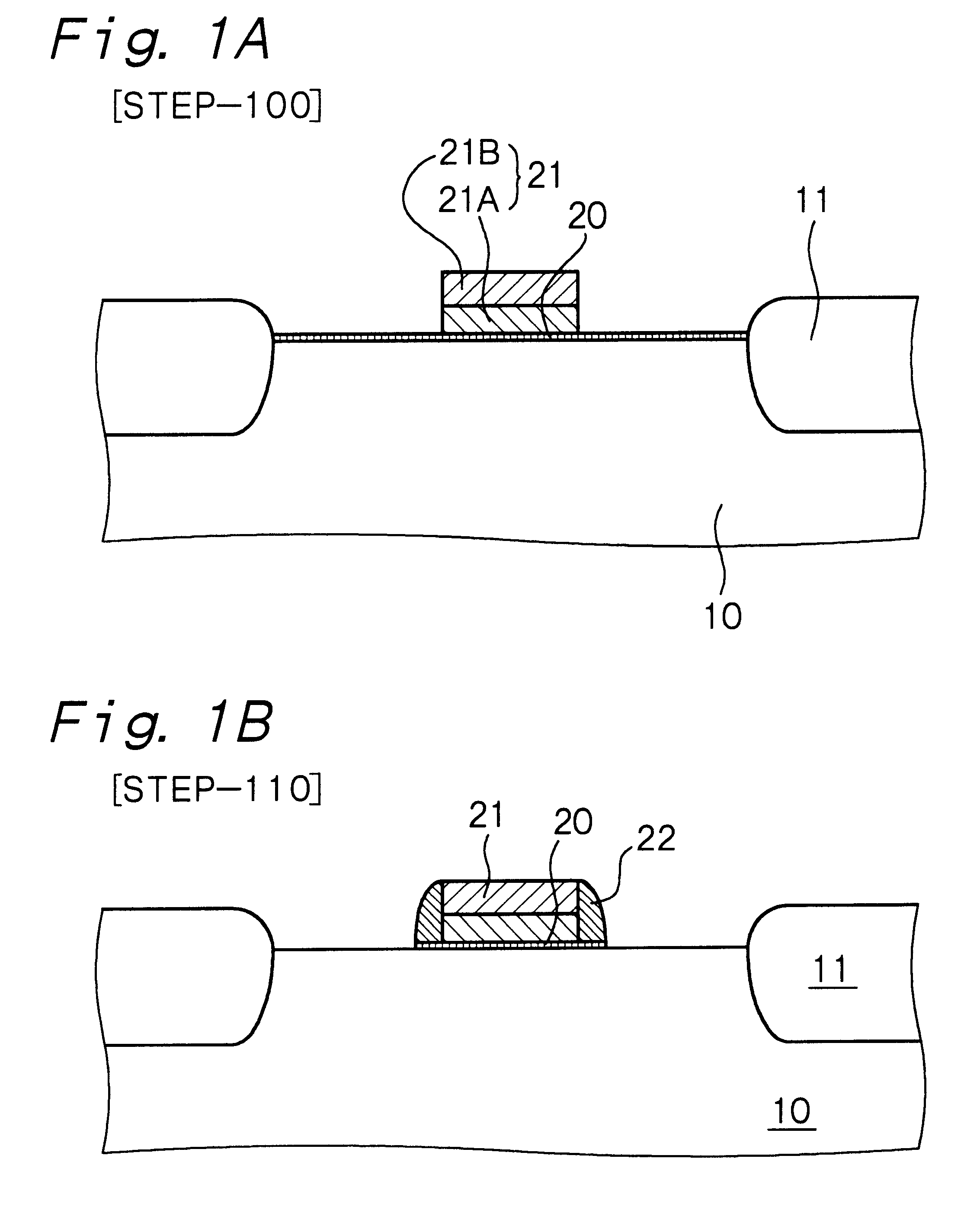
A gate insulating layer 20 is formed on a surface of a silicon semiconductor substrate 10 corresponding to a semi-conductive layer, and a gate electrode 21 is formed on the gate insulating layer 20, in the same manner as in [Step-100] of Example 1. Unlike Example 1, the gate electrode 21 is formed of a polysilicon layer alone in Example 2.
[Step-210]
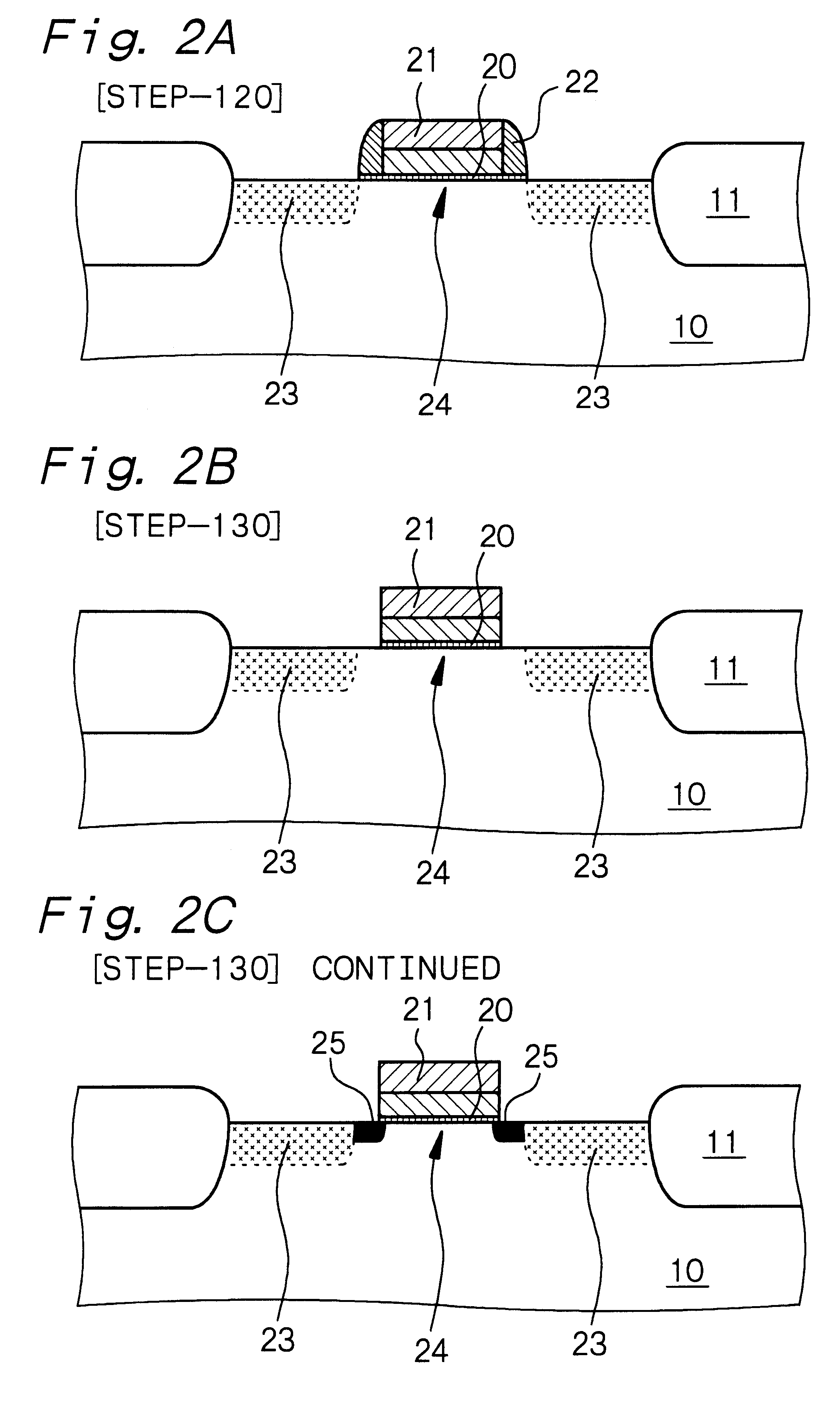
Then, [Step-110], [Step-120] and [Step-130] in Example 1 are carried out, whereby a structure shown in FIG. 4A can be obtained.
[Step-220]
Then, gate-side-walls 30 are formed on ...
example 3
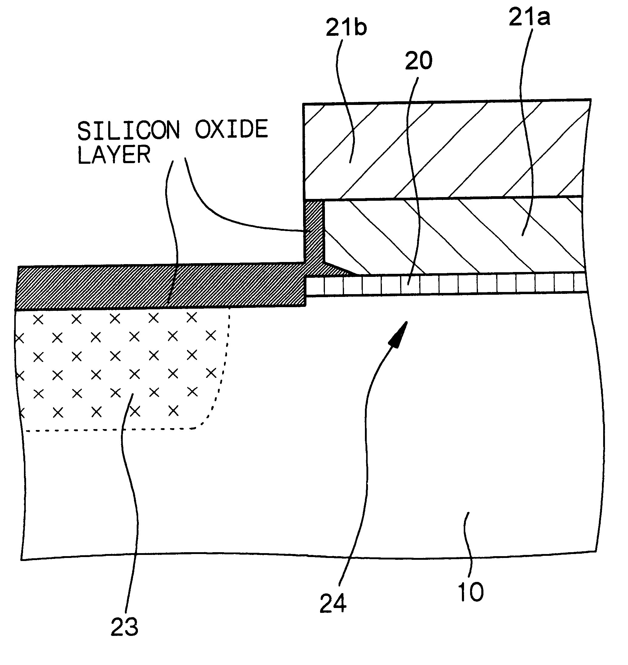
Example 3 is also a variant of Example 1. Example 3 differs from Example 1 in that the formation of extension regions is carried out from a source / drain region side a plurality of times. The method for producing a semiconductor device in Example 3 will be explained with reference to schematic partial cross-sectional views of a silicon semiconductor substrate, etc., shown in FIGS. 5A, 5B, 6A, 6B, 7A and 7B.
[step-300]
A gate insulating layer 20 is formed on a surface of a silicon semiconductor substrate 10 corresponding to a semi-conductive layer, and a gate electrode 21 is formed on the gate insulating layer 20, in the same manner as in [Step-100] of Example 1.
[Step-310]
Then, sidewalls having a multi-layered structure are formed on side walls of the gate electrode 21. For this purpose, first, an approximately 10 nm thick SiO.sub.2 layer (not shown) is deposited on the entire surface by a TEOS-CVD method. Then, a 50 nm thick polysilicon layer is deposited on the entire surface by a CVD...
PUM
 Abstract
Description
Claims
Application Information
 - R&D
- Intellectual Property
- Life Sciences
- Materials
- Tech Scout
- Unparalleled Data Quality
- Higher Quality Content
- 60% Fewer Hallucinations
Browse by: Latest US Patents, China's latest patents, Technical Efficacy Thesaurus, Application Domain, Technology Topic, Popular Technical Reports.
© 2025 PatSnap. All rights reserved.Legal|Privacy policy|Modern Slavery Act Transparency Statement|Sitemap|About US| Contact US: help@patsnap.com