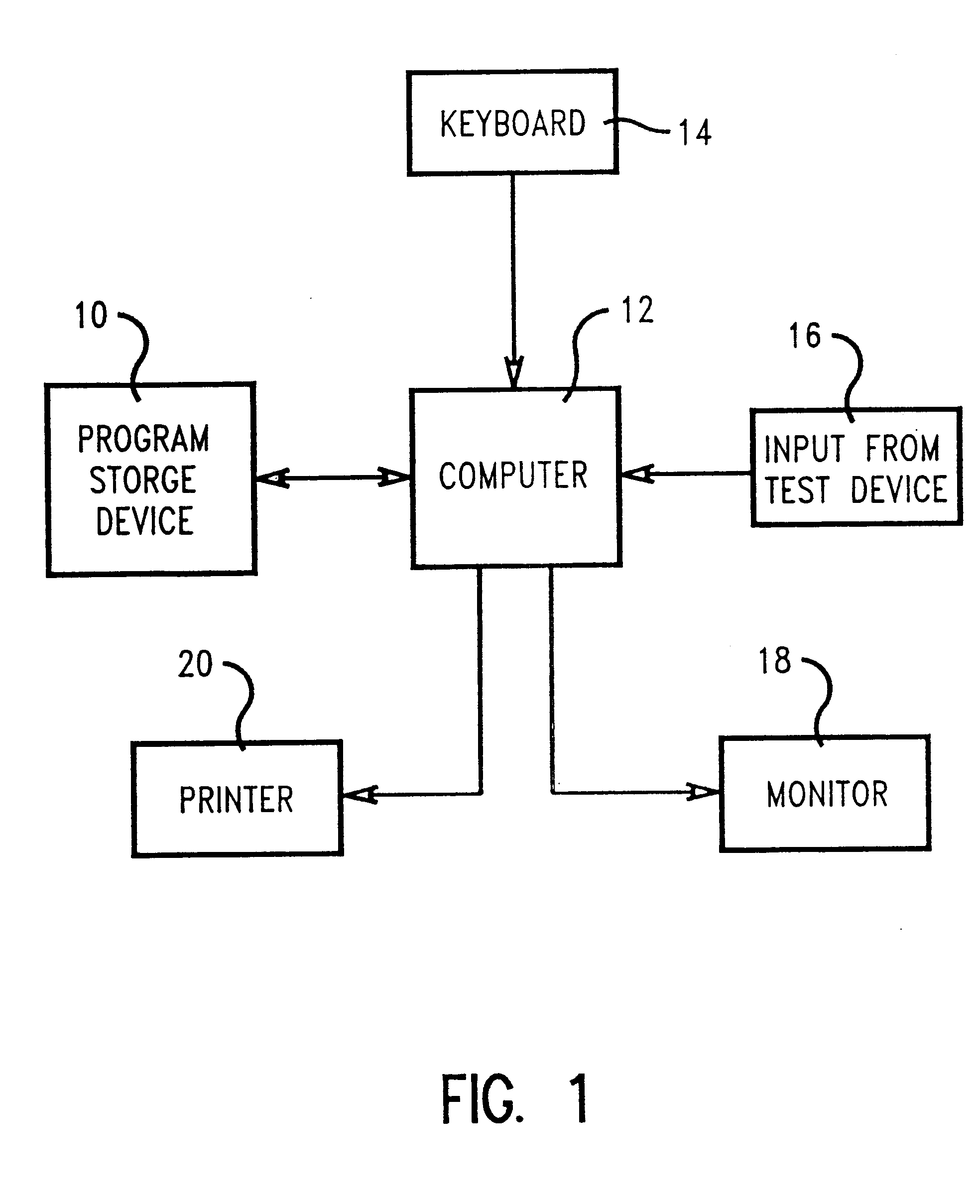
Method of determining model parameters for a MOSFET compact model using a stochastic search algorithm
a compact model and model parameter technology, applied in the field of semiconductor devices, can solve the problems of inability of model software to provide a measure of the fit of the overall model, inability to evaluate the reasonableness of values beyond, and additional iterations are required, so as to limit the size of the search space
- Summary
- Abstract
- Description
- Claims
- Application Information
AI Technical Summary
Benefits of technology
Problems solved by technology
Method used
Image


Examples
example
Initial Lab Measurements
A set of 10-16 individual MOSFETs were processed on the same die with different channel lengths and widths and selected for measurement. These MOSFETs of differing geometries were selected to include a device long and wide enough so that short channel and narrow channel effects are negligible, a series of devices of this same length but decreasing widths down to the minimum width allowed by the technology ground rules, a series of devices of this same width but decreasing lengths down to the minimum length allowed by the technology ground rules, and one of more devices that exhibit a combination of short and narrow channel effects.
Three sets of device current measurements were made. All measured data, except those below measurement capability of the instruments, were kept for model verification. In order to reduce the run time of the fitting program, only a subset of the measured data is used for fitting.
In the first set, drain current Id as a function of gat...
PUM
 Abstract
Description
Claims
Application Information
 - R&D
- Intellectual Property
- Life Sciences
- Materials
- Tech Scout
- Unparalleled Data Quality
- Higher Quality Content
- 60% Fewer Hallucinations
Browse by: Latest US Patents, China's latest patents, Technical Efficacy Thesaurus, Application Domain, Technology Topic, Popular Technical Reports.
© 2025 PatSnap. All rights reserved.Legal|Privacy policy|Modern Slavery Act Transparency Statement|Sitemap|About US| Contact US: help@patsnap.com