
Passive sample and hold in an active switched capacitor circuit

a switched capacitor and passive sample technology, applied in the field of switching capacitor circuits, can solve the problems of increasing the critical issue of package power dissipation, requiring a large area, and requiring power-consuming operational amplifiers, and achieve the effect of less area

Inactive Publication Date: 2001-11-06
AVAGO TECH INT SALES PTE LTD
View PDF12 Cites 9 Cited by
  • Summary
  • Abstract
  • Description
  • Claims
  • Application Information

AI Technical Summary

Benefits of technology

It is a further object of an embodiment of the present invention to provide a switched capacitor circuit that is configured to perform a sample and hold with frequency shaping operation, and consumes less area.

Problems solved by technology

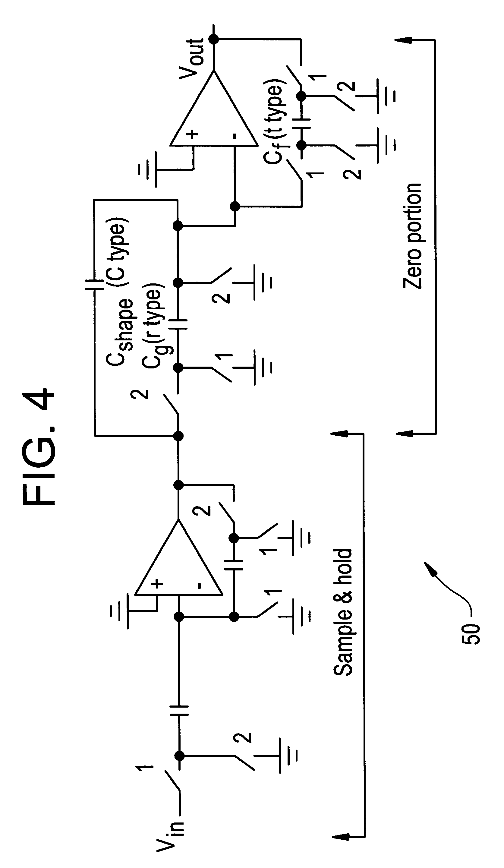
As shown, two active stages are implemented (the sample and hold portion and the zero portion), and each requires a large area, power-consuming operational amplifier.
For example, with regard to Ethernet chips, as the number of required ports (i.e., channels) continue to increase, package power dissipation is becoming more and more of a critical issue.

Method used


Image

  • Passive sample and hold in an active switched capacitor circuit
  • Passive sample and hold in an active switched capacitor circuit
  • Passive sample and hold in an active switched capacitor circuit

Examples


Embodiment Construction

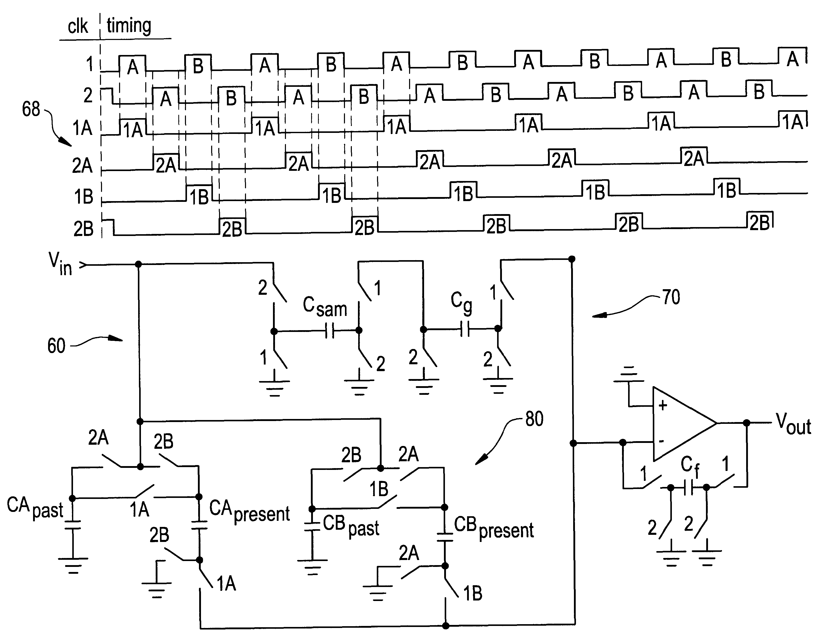
FIG. 5 illustrates a switched capacitor circuit 60 including a sample and hold in accordance with an embodiment of the present invention. The sample and hold does not require a pair of large area, power-consuming operational amplifiers and, as such, consumes less power and less area.

Also shown in FIG. 5 are waveforms 68 corresponding to clock signals which control the switches included in the circuit. Specifically, waveforms corresponding to two clock signals, "1" and "2", are illustrated, and waveforms corresponding to other four signals, "1A" , "2A", "1B" and "2B", that are derived from clock signals "1" and "2" are shown. Preferably, clock signals "1" and "2" are approximately 48% duty cycle, non-overlapping clock signals, and clock signals "1A", "2A", "1B" and "2B" are approximately 24% duty cycle, non-overlapping clock signals derived from clock signals "1" and "2". It should be noted that the "B" in "1B" and "2B" does not indicate a complement signal or "bar." The circuit illu...


PUM


Abstract

A sample and hold in a switched capacitor circuit with frequency shaping. The sample and hold does not require a pair of large area, power-consuming operational amplifiers and, as such, consumes less power and less area. Preferably, the sample and hold is operable in four different states wherein a different set of switches are closed in each of the four states. The switches are controlled by two clock signals and a plurality of signals derived from the two clock signals, such as four signals derived from the two clock signals. Desirably, the sample and hold with frequency shaping is configured to sample a voltage across a first capacitor while a second capacitor is disconnected from said first capacitor, and is configured to thereafter connect the second capacitor to the first capacitor and possibly discharge at least a portion of a charge held in the first capacitor into the second capacitor.

Description

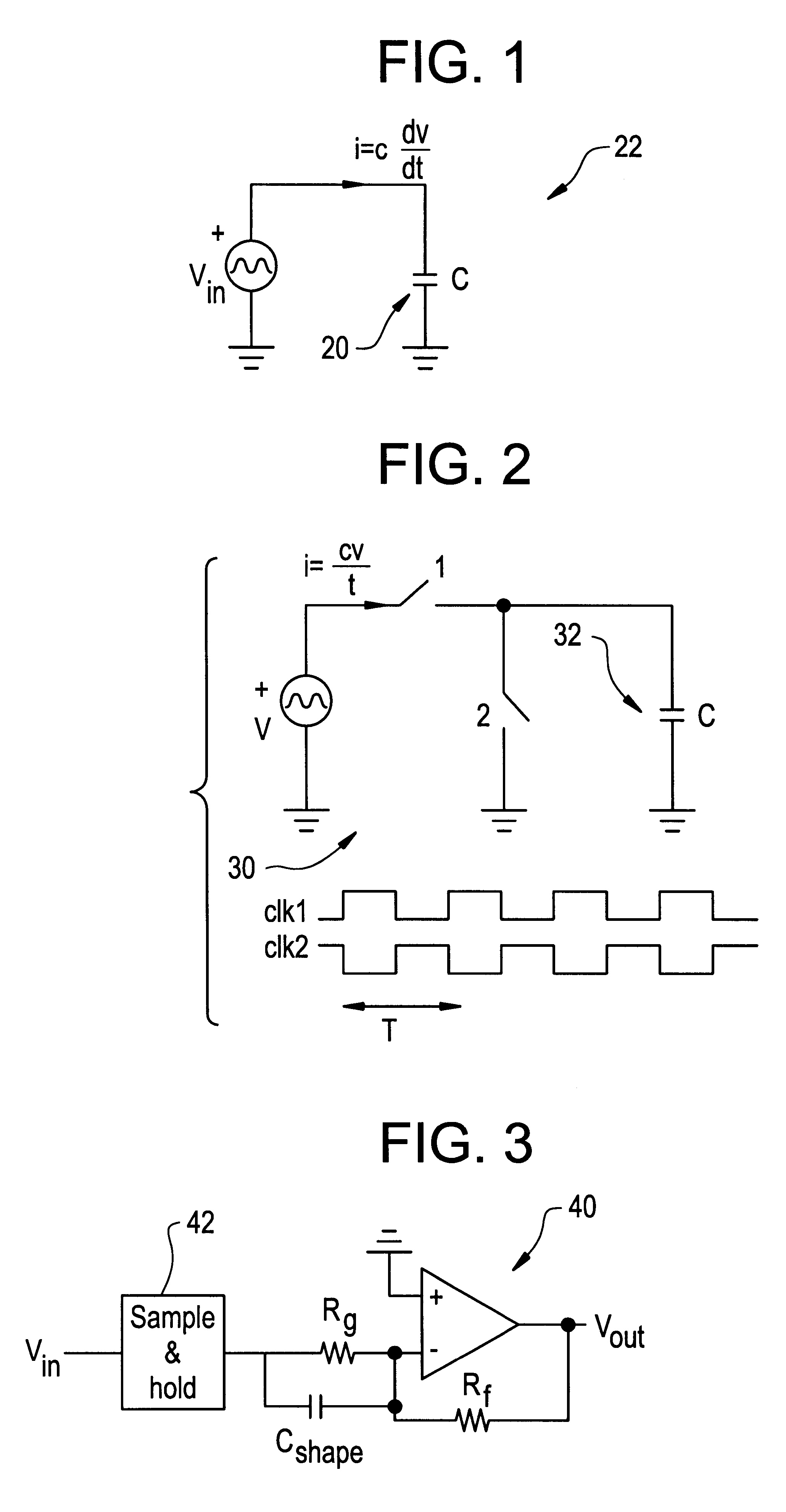
Each capacitor in a switched capacitor circuit can be described as acting either as a capacitor or as a resistor. A capacitor in a switched capacitor circuit is said to act as a capacitor when the capacitor has memory of a previous value, and passes current that is proportional to dv / dt (i.e., I (current)=Cdv / dt). Such a capacitor generally performs some type of frequency shaping because the capacitor passes more and more current as the frequency of the voltage increases across the terminals of the capacitor. In contrast, a capacitor in a switched capacitor circuit is said to act as a resistor when the capacitor has no memory of a previous value, and passes current that is proportional to a voltage (i.e., V=iR (voltage=current*resistance), or equivalently I=CV / T (wherein T is the period of a sampling clock)).Unlike with a capacitor, the value of the current passed by a true resistor is independent of the frequency of the input signal. FIG. 1 illustrates a circuit 20 wherein the capa...

Claims


Application Information

Patent Timeline
Patent Type & Authority Patents(United States)
IPC IPC(8): G11C27/00G11C27/02H03H19/00
CPCG11C27/026H03H19/004
Inventor SAVAGE, SCOTT C.
Owner AVAGO TECH INT SALES PTE LTD
Learn More