
Methods and devices related to electrodes for p-type group III nitride compound semiconductors

a compound semiconductor and nitride technology, applied in semiconductor devices, semiconductor/solid-state device details, electrical apparatus, etc., can solve the problems of poor adhesion strength between the au and the gan layer, poor ohmic characteristic of the semiconductor, and peeling of the electrode layer

Inactive Publication Date: 2000-09-19
TOYODA GOSEI CO LTD
View PDF11 Cites 39 Cited by
  • Summary
  • Abstract
  • Description
  • Claims
  • Application Information

AI Technical Summary

Benefits of technology

The resulting metal electrode has a double layer structure comprising a first metal electrode layer and a second metal electrode layer. Because the element of the first metal electrode layer has an ionization potential that is lower than that of the element of the second metal electrode layer, the first metal electrode layer has a greater adhesive strength than the second metal electrode layer. The second metal electrode layer, which has a work function that is larger than that of the first metal electrode layer, or which has a higher ionization potential than that of the first metal electrode layer, has a good ohmic characteristic to the Group III nitride compound semiconductor. Carrying out heat treatment on the electrode causes the element of the first electrode layer to move to the surface of the second metal electrode layer. In particular, the element of the second metal electrode layer penetrates through the first electrode layer and significantly into the Group III nitride compound semiconductor. A larger portion of the element of the first metal electrode layer moves and distributes on the surface of the electrode. This reversing of the distribution of the elements of the first and the second metal electrode layers improves both adhesive strength and ohmic characteristics between the electrode and the Group III nitride compound semiconductor.
A study of what causes the reversing of the distribution of the elements of the first and the second metal electrode layers was conducted and it was concluded that depositing a metal layer that has a relatively lower ionization potential as the first metal electrode layer, depositing another metal layer having a relatively better ohmic characteristic as the second metal electrode layer, and carrying out heat treatment within a predetermined temperature range under low vacuum causes the reversing of the distribution of the elements of the first and the second metal electrode layers. Because the element of the second metal electrode layer penetrates significantly into the Group III nitride compound semiconductor, the ohmic characteristic between the electrode and the Group III nitride compound semiconductor, as a whole, is improved. Further, because the first metal electrode layer includes a metal that has a relatively lower ionization potential, stronger adhesive strength to the Group III nitride compound semiconductor is brought about. As a result of the foregoing, a semiconductor device that has both a strong adhesive and a good ohmic characteristics is obtained.
When, for example, nickel (Ni) is used as the first metal electrode layer and gold (Au) is used as the second metal electrode layer, the gold penetrates through the Ni first metal electrode layer. In sum, the ohmic characteristic is improved by using gold (Au) and the adhesive strength between the electrode to the semiconductor layer is maintained by using nickel (Ni).
A Group III nitride compound semiconductor device having an electrode formed of the double layer structure described above improves the devices characteristics. For example, less voltage needs to be applied and there is less resistivity. In addition, when an electrode formed of the double layer structure described above is used for a LED or a LD, emission efficiency is improved.

Problems solved by technology

However, because the adhesive strength between the Au and the GaN layer is poor, an electrode layer made of Au peels easily away from the GaN layer during alloying processes performed on the GaN layer.
Nickel (Ni) is interposed between the Au electrode layer and the GaN layer so as to improve the adhesive strength, This arrangement, however, leads to poor ohmic characteristic of the semiconductor and high contact resistance between the GaN layer and the Ni.

Method used


Image

  • Methods and devices related to electrodes for p-type group III nitride compound semiconductors
  • Methods and devices related to electrodes for p-type group III nitride compound semiconductors
  • Methods and devices related to electrodes for p-type group III nitride compound semiconductors

Examples


example

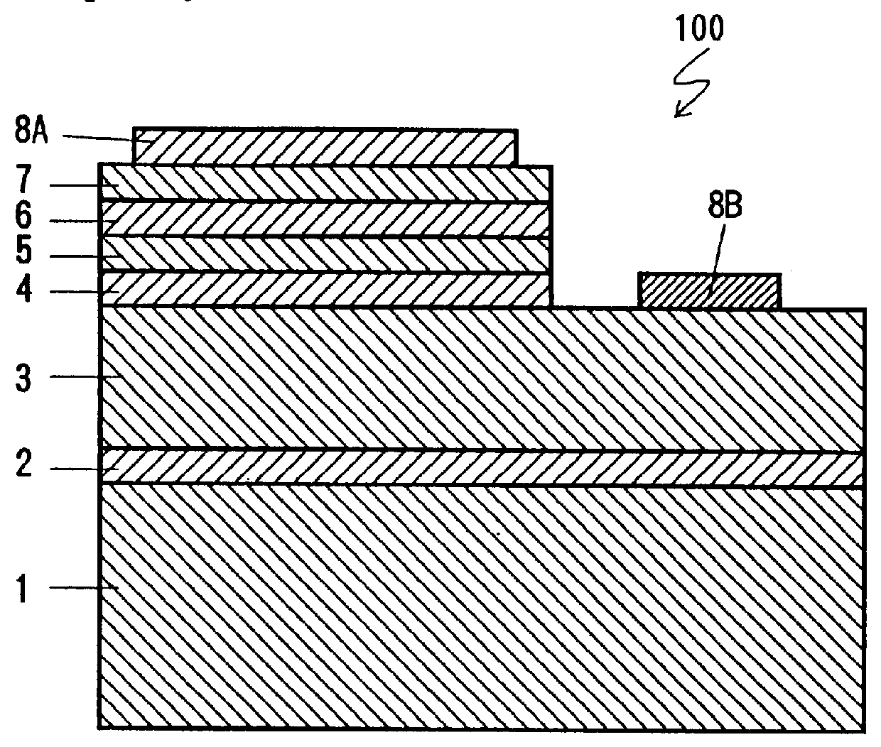
FIG. 1 shows a sectional view of a LED 100 made of Group III nitride compound semiconductor that has been formed on a sapphire substrate 1. The Group III nitride compound semiconductor can satisfy the formula: Al.sub.x Ga.sub.y In.sub.1-x-y N, wherein 0.ltoreq.x.ltoreq.1, 0.ltoreq.y.ltoreq.0, and 0.ltoreq.x-y.ltoreq.1. An AlN buffer layer 2 is formed on the sapphire substrate 1 and an silicon (Si) doped gallium nitride (GaN) layer 3 of n.sup.+ -type is formed on the AlN buffer layer 2. An undoped n-layer 4, comprising of Al.sub.0.1 Ga.sub.0.9 N and having a thickness generally of 0.5 .mu.m, is formed on the n'-layer 3. A magnesium (Mg) doped GaN layer, or active layer 5, having a thickness generally of 0.4 .mu.m, is formed on the n-layer 4. An Mg-doped Al.sub.0.1 Ga.sub.0.9 N layer 6, having p-type conduction and having a thickness generally of 0.2 .mu.m, is formed on the active layer 5. A highly Mg-doped p.sup.+ -layer 7, comprised of GaN and having a thickness generally of 0.15 .m...


PUM


Abstract

An electrode for a Group III nitride compound semiconductor having p-type conduction that has a double layer structure. The first metal electrode layer comprising, for example, nickel (Ni) and the second metal electrode layer comprising, for example, gold (Au). The Ni layer is formed on the Group III nitride compound semiconductor having p-type conduction, and the Au layer is formed on the Ni layer. Heat treatment changes or reverses the distribution of the elements Ni and Au. Namely, Au is distributed deeper into the Group III nitride compound semiconductor than is Ni. As a result, the resistivity of the electrode is lowered and its ohmic characteristics are improved as well as its adhesive strength.

Description

1. Field of the InventionThe present invention relates to electrodes for a Group III nitride compound semiconductor having p-type conduction, a Group III nitride compound semiconductor device having this type of electrodes, and methods of forming these electrodes. Especially, the invention relates to electrodes for a Group III nitride compound semiconductor having p-type conduction with improved ohmic characteristics, adhesive strength and contact resistance between the semiconductor and the electrodes.2. Description of Background InformationConventionally, gold (Au) that is deposited on a surface of a p-type conductive gallium nitride (GaN) layer is used as an electrode. However, because the adhesive strength between the Au and the GaN layer is poor, an electrode layer made of Au peels easily away from the GaN layer during alloying processes performed on the GaN layer.Nickel (Ni) is interposed between the Au electrode layer and the GaN layer so as to improve the adhesive strength, ...

Claims


Application Information

Patent Timeline
IPC IPC(8): H01L21/02H01L21/285H01L29/45H01L29/40H01L33/00H01L33/32H01L33/40
CPCH01L21/28575H01L29/452H01L33/40H01L33/32
Inventor SHIBATA, NAOKIUMEZAKI, JUNICHIASAI, MAKOTOUEMURA, TOSHIYAKOZAWA, TAKAHIROMORI, TOMOHIKOOHWAKI, TAKESHI
Owner TOYODA GOSEI CO LTD
Learn More