CDMA communication method and group spreading modulator
a communication method and group spreading technology, applied in the field of cdma (code division multiple access) communication methods and group spreading modulators, can solve the problems of degradation of transmission quality, equal transmission rate for the entire simultaneous user,
- Summary
- Abstract
- Description
- Claims
- Application Information
AI Technical Summary
Problems solved by technology
Method used
Image
Examples
embodiment 2
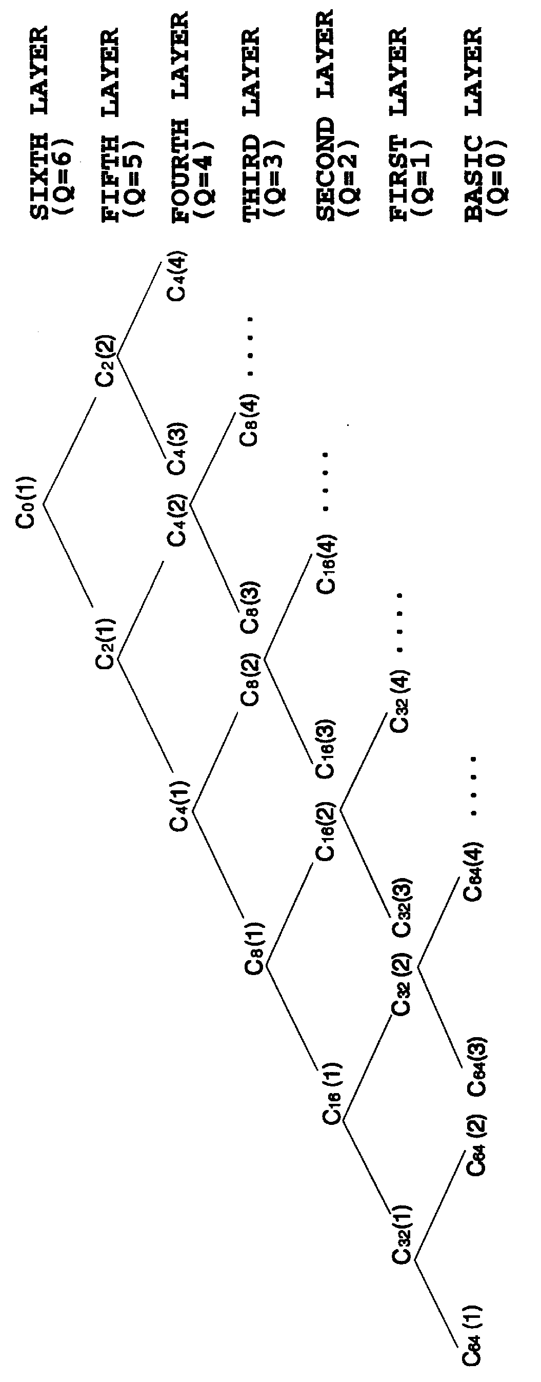
FIG. 9 shows a configuration of a modulator that can implement multi-rate modulation using the spreading sequences of the tree structure as shown in FIG. 3.
The modulator as shown in FIG. 9 has, besides the configuration as shown in FIG. 7, a structure that enables the narrowband modulation signals to be input directly to the input terminals of upper layers. To achieve this, each of the two inputs of the basic modulator element is provided with a switch for switching the inputs. For example, a modulation signal of a channel of twice the symbol rate can be directly input to one of the two inputs of the element at the secondary layer, which includes that channel. Likewise, a modulation signal of a channel of four times the symbol rate can be directly input to one of the two input terminals of the element at the third layer, the one of the two input terminals including that channel, and a modulation signal of a channel of the 2.sup.P times the symbol rate can be directly input to one of...
embodiment 3
FIG. 10 shows a group modulator constructed using a smaller number of basic modulator elements than that of FIG. 7. In FIG. 10, the basic modulator elements are hierarchically connected in R layers, where R is less than N, and the output of the topmost element is multiplied by an orthogonal code sequence with a period of 2.sup.(N-R) chip intervals, thus constituting a group modulator unit. At the final layer, the outputs of the 2.sup.(N-R) group modulator units are summed up. The configuration as shown in FIG. 10 is a case where N=6 and R=3.
In the configuration as shown in FIG. 10, the elements are hierarchically connected in R layers (R<N) rather than connected in N layers as shown in FIG. 7, and the output of the topmost element is multiplied by an orthogonal spreading code sequence with the 2.sup.(N-R) chip intervals by a multiplier 103. The total of 2.sup.(N-R) thus constructed group modulator units 102 are used so that their outputs are summed up by the adder 101, thereby produ...
embodiment 4
FIG. 11 shows another configuration of an 2.sup.R channel group modulator corresponding to that enclosed by the broken lines in FIG. 10. In FIG. 11, the user data of 2.sup.R channels are each input to data modulators 112 to obtain narrowband modulated signals. The 2.sup.R data modulated signal outputs from the data modulators 112 are multiplied by spread sequences fed from a low rate orthogonal periodic spreading sequence generator 114 by multipliers 116, and combined by an adder 117. Subsequently, the output of the adder 117 is multiplied by a orthogonal spreading code sequence with a period of an 2.sup.(N-R) chip interval as in FIG. 10. The spreading sequences to be multiplied by the modulated signal outputs will now be described below.
The spread modulation as shown in FIG. 11 carries out multiplication by the orthogonal codes through two steps. First, the spreading codes generated by the low rate orthogonal periodic spreading sequence generator 114 are multiplied which constitute...
PUM
 Abstract
Description
Claims
Application Information
 - R&D
- Intellectual Property
- Life Sciences
- Materials
- Tech Scout
- Unparalleled Data Quality
- Higher Quality Content
- 60% Fewer Hallucinations
Browse by: Latest US Patents, China's latest patents, Technical Efficacy Thesaurus, Application Domain, Technology Topic, Popular Technical Reports.
© 2025 PatSnap. All rights reserved.Legal|Privacy policy|Modern Slavery Act Transparency Statement|Sitemap|About US| Contact US: help@patsnap.com


