Process for fabricating circuitry on substrates having plated through-holes

a technology of through-hole plated circuitry and substrate, which is applied in the direction of resistive material coating, cable/conductor manufacturing, metallic material coating process, etc., can solve the problems of relatively thick film resist, thin photoresist layer not being able to tent or protect the through-hole, and insufficient geometries for new substrate requirements

Inactive Publication Date: 2000-01-11
IBM CORP
View PDF9 Cites 24 Cited by
  • Summary
  • Abstract
  • Description
  • Claims
  • Application Information

AI Technical Summary

Problems solved by technology

However, these geometries are not sufficient for the new substrate requirements.
However, these thin photoresist layers are not capable of tenting or protecting plated through-holes that might exist on the printed circuit board or card.
On the other hand, re

Method used


Image

  • Process for fabricating circuitry on substrates having plated through-holes
  • Process for fabricating circuitry on substrates having plated through-holes
  • Process for fabricating circuitry on substrates having plated through-holes

Examples


Embodiment Construction

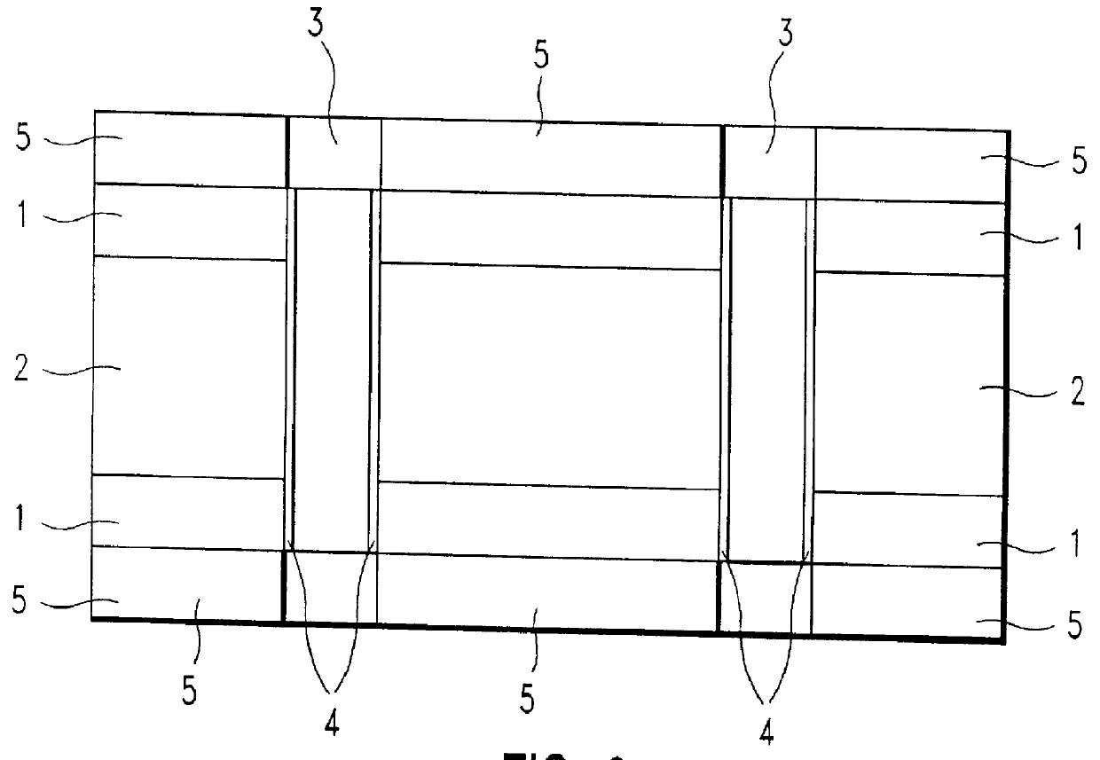
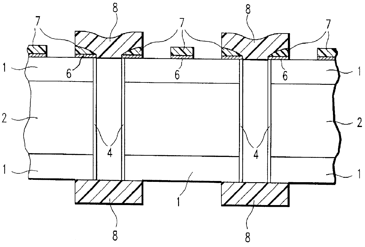
In order to facilitate an understanding of the present invention, reference will be made to the drawing which schematically illustrates a procedure for providing fine line circuitization of substrates with plated through-holes without concomitantly jeopardizing the integrity of the plated through-holes.

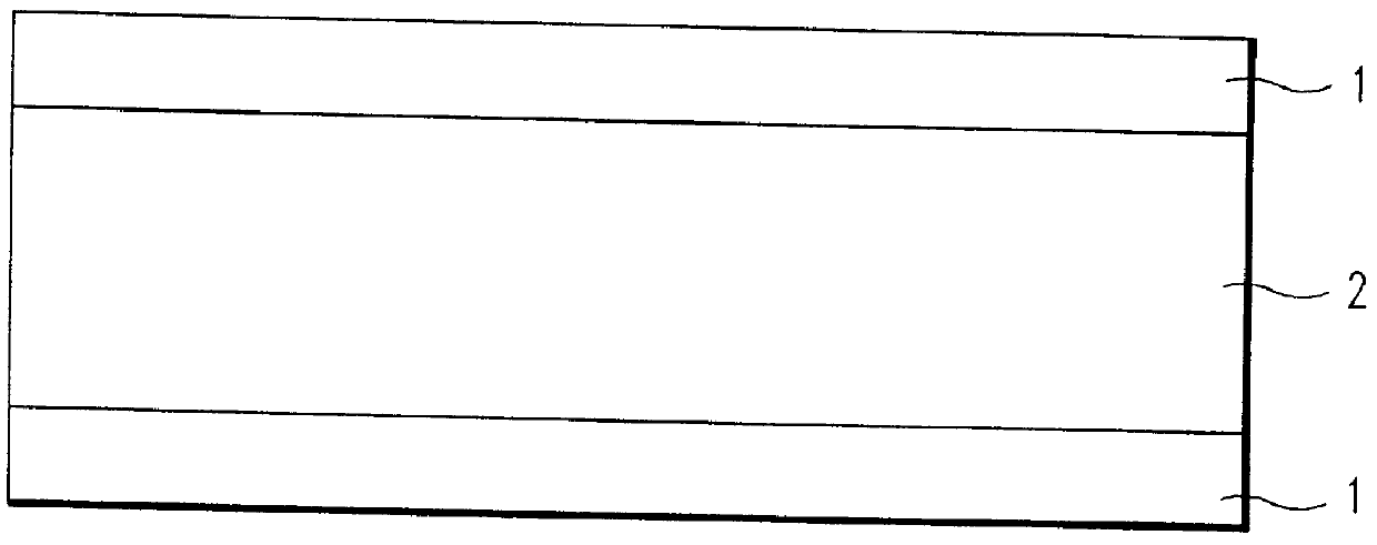
A copper foil 1 is laminated to a dielectric substrate material 2 (see FIG. 1). The dielectric substrate material includes both thermoplastic and thermosetting polymers and preferably thermosetting polymers. Typical thermosetting polymeric materials to which the copper foil is laminated include epoxy, phenolic base materials, and polyimides. The dielectric materials may be molded materials of a polymer containing fillers and / or reinforcing agents such as glass filled epoxy or phenolic base materials. Examples of some phenolic type materials include copolymers of phenol, resorcinol and cresol. Examples of some suitable thermoplastic polymeric materials include polyolefins, such as poly...


PUM

PropertyMeasurementUnit
Lengthaaaaaaaaaa
Lengthaaaaaaaaaa
Thicknessaaaaaaaaaa

Abstract

Circuitry is formed on a substrate having at least one plated through-hole employing two different photoresist materials. A first photoresist is applied on a conductive layer located on a substrate and is developed to define a desired conductive circuit pattern. A second photoresist is laminated onto the structure and is developed so that the second photoresist material remains in the vicinity of the through-hole. The conductive layer is etched to provide the desired circuit pattern, and the remaining portions of the second and first photoresists are removed.

Description

DESCRIPTION1. Technical FieldThe present invention is concerned with a process for providing circuitry on substrates having plated through holes. The present invention is especially advantageous for providing fine line circuitry. More particularly, the present invention provides the desired circuitry while at the same time protects the plated through-holes during the processing.2. Background of InventionA printed circuit board or card serves as a support substrate for various individual electronic components such as integrated circuits, resistors, and capacitors. The printed circuit board or card also provides the metallic conductors for conveying electrical current between the connected terminals of the electronic components. In addition, conductors on opposite sides of the board or card are frequently connected by plated through-holes. Plated through-holes are created by plating copper or some other metal onto the side walls of the through-holes formed through the circuit board or...

Claims


Application Information

Patent Timeline
IPC IPC(8): G03F7/00H05K3/00H05K3/06H05K3/42
CPCG03F7/0035H05K3/0094H05K3/064H05K3/427H05K2203/0588H05K2203/068H05K2203/1394H05K2203/1572
Inventor SEBESTA, ROBERT DAVIDWILSON, JAMES WARREN
Owner IBM CORP
Why Eureka
Try Eureka