
Flash memory storage apparatus and a biasing method thereof, which can reduce a gate induced drain leakage (GIDL) and improve reliability of memory cells

a flash memory and biasing technology, applied in the field of flash memory storage apparatus and an operating method thereof, can solve problems such as reducing the reliability of flash memory cells

Inactive Publication Date: 2022-11-17
POWERCHIP SEMICON MFG CORP
View PDF2 Cites 0 Cited by
  • Summary
  • Abstract
  • Description
  • Claims
  • Application Information

AI Technical Summary

Benefits of technology

The patent is about a flash memory storage device and a method to improve its reliability by reducing a particular effect called gate induced drain leakage (GIDL). The device uses a voltage generating circuit to apply different bias voltages to the word lines to achieve this. The technical effect is to improve the reliability of the memory cells.

Problems solved by technology

However, during programming, gate induced drain leakage (GIDL) affects the state of data stored in the flash memory cells, leading to the reduction of reliability of the flash memory cells.

Method used


Image

  • Flash memory storage apparatus and a biasing method thereof, which can reduce a gate induced drain leakage (GIDL) and improve reliability of memory cells
  • Flash memory storage apparatus and a biasing method thereof, which can reduce a gate induced drain leakage (GIDL) and improve reliability of memory cells
  • Flash memory storage apparatus and a biasing method thereof, which can reduce a gate induced drain leakage (GIDL) and improve reliability of memory cells

Examples


Embodiment Construction

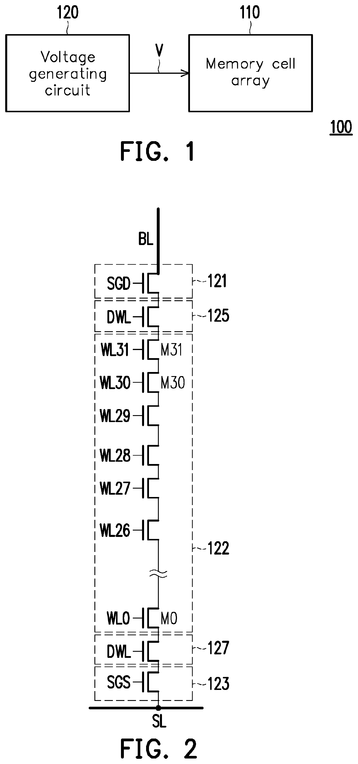
[0028]FIG. 1 is a schematic diagram briefly illustrating a flash memory storage apparatus according to an embodiment of the disclosure. FIG. 2 is a schematic diagram briefly illustrating the memory cell string according to the embodiment depicted in FIG. 1. With reference to FIG. 1 and FIG. 2, a flash memory storage apparatus 100 provided in the embodiment includes a memory cell array 110 and a voltage generating circuit 120. The voltage generating circuit 120 is coupled to the memory cell array 110. In this embodiment, the flash memory storage apparatus 100 is, for instance, a NAND gate flash memory. The voltage generating circuit 120 may have a circuit design method well known to those skilled in the art.

[0029]The memory cell array 110 includes a bit line BL, a source line SL, and word lines WL0 to WL31. The memory cell array 110 further includes at least one memory cell string 122. The memory cell string 122 is coupled between the bit line BL and the source line SL. The memory ce...


PUM


Abstract

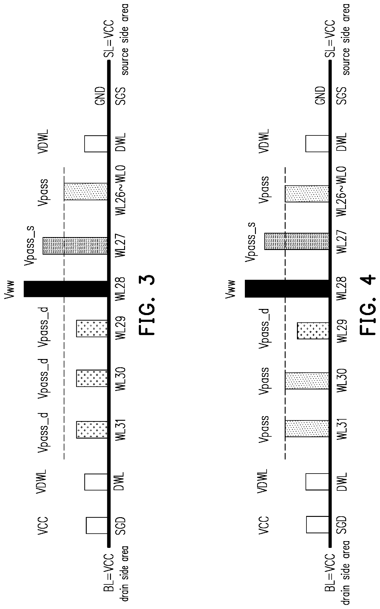
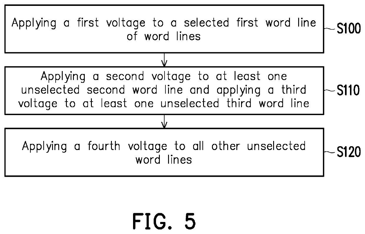
A flash memory storage apparatus includes a memory cell array and a voltage generating circuit. The memory cell array includes at least one memory cell string coupled between a bit line and a source line and including memory cells; each memory cell is coupled to a corresponding word line. The voltage generating circuit is coupled to the memory cell array and configured to output a bias voltage to the word line. A first voltage is applied to a selected word line. A second voltage and a third voltage are applied to unselected second and third word lines, respectively. The first voltage is greater than the second voltage, and the second voltage is greater than the third voltage. The second word line and the third word line are located on two sides of the first word line. A biasing method of a flash memory storage apparatus is also provided.

Description

CROSS-REFERENCE TO RELATED APPLICATION[0001]This application is a continuation application of and claims the priority benefit of U.S. application Ser. No. 17 / 204,955, filed on Mar. 18, 2021, now pending, which claims the priority benefit of Taiwan patent application serial no. 110104200, filed on Feb. 4, 2021. The entirety of each of the above-mentioned patent applications is hereby incorporated by reference and made a part of this specification.BACKGROUNDTechnical Field[0002]The disclosure relates to a memory storage apparatus and an operating method thereof, and particularly relates to a flash memory storage apparatus and a biasing method thereof.Description of Related Art[0003]With the evolution of electronic technologies, electronic apparatuses have become indispensable tools in people's lives. Flash memories which can perform long-term data storage functions and have large storage capacity have become important data storage media. The flash memory contains a plurality of flash ...

Claims


Application Information

Patent Timeline
Patent Type & Authority Applications(United States)
IPC IPC(8): G11C11/408G11C11/4074G11C11/4094G11C16/06G11C16/34G11C16/08G11C16/04
CPCG11C11/4085G11C11/4074G11C11/4094G11C16/06G11C16/3418G11C16/3427G11C16/08G11C16/0483G11C16/3422G11C16/24G11C16/34G11C16/10
Inventor LIEN, CHIEN-HUNGWANG, CHIH-YUAN
Owner POWERCHIP SEMICON MFG CORP
Learn More