Process for protecting an upper stage of electronic components of an integrated circuit against antenna effects

a technology of electronic components and integrated circuits, which is applied in the direction of semiconductor devices, semiconductor/solid-state device details, diodes, etc., can solve the problems of not providing entirely satisfactory unable to effectively drain electric charges to the upper substrate, and prior-art solutions that do not provide complete protection of the upper stage of electronic components c against antenna effects

Pending Publication Date: 2022-09-15
COMMISSARIAT A LENERGIE ATOMIQUE ET AUX ENERGIES ALTERNATIVES
View PDF0 Cites 0 Cited by
  • Summary
  • Abstract
  • Description
  • Claims
  • Application Information

AI Technical Summary

Benefits of technology

[0037]By “bulk substrate”, what is meant is a substrate possessing a single constituent material.
[0038]By “SOI”, what is meant is silicon-on-insulator, i.e. a substrate of silicon / insulator / silicon type.
[0039]The term “substrate” designates the first substrate (the second substrate, respectively) when it is a question of an electronic component of the first stage (of the second stage, respectively).
[0040]Thus, such electronic components are particularly subject to antenna effects because of the presence of a thin oxide layer.
[0041]According to one feature of the invention, steps a) and b) are executed so that the first and second substrates are silicon wafers.
[0042]According to one feature of the invention, step a) comprises the steps:

Problems solved by technology

Thus, electric charges will accumulate and eventually damage the oxide layer Ox, most particularly when the oxide layer Ox is thin.
These prior-art solutions do not provide entirely satisfactory protection of the upper stage of electronic components C against antenna effects, in the case of 3D integration.
Specifically, solutions (i) and (ii) do not allow electric charges to be effectively drained to the upper substrate and then to the biasing electrode E1.
Solution (iii) requires, for its part, vast resources in terms of interconnect lines, and it is therefore not desirable for VLSI.

Method used


Image

  • Process for protecting an upper stage of electronic components of an integrated circuit against antenna effects
  • Process for protecting an upper stage of electronic components of an integrated circuit against antenna effects

Examples


Embodiment Construction

[0057]For the sake of simplicity, elements that are identical or that perform the same function in the various embodiments have been designated with the same references.

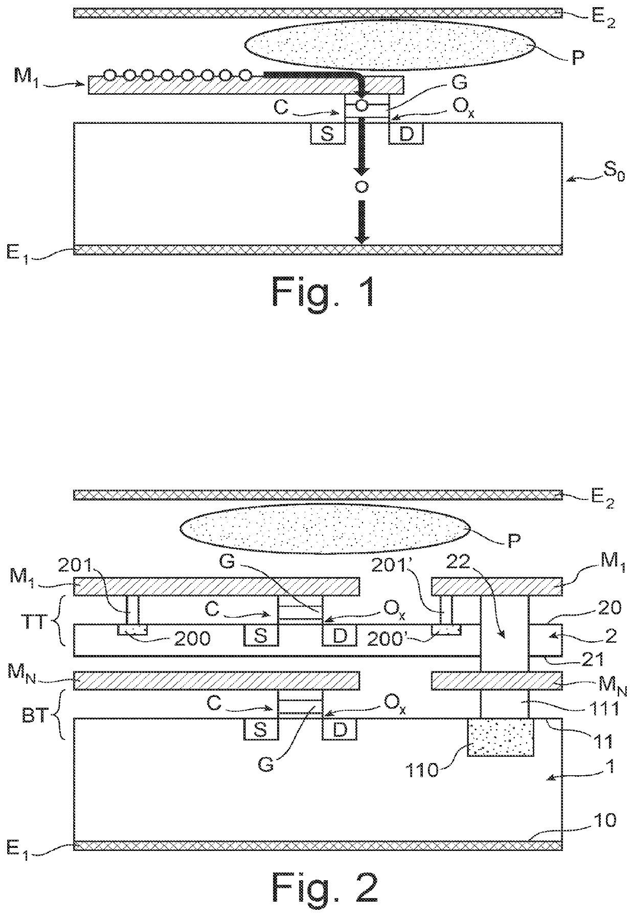
[0058]One subject of the invention is a process for protecting an upper stage TT of electronic components C of an integrated circuit against antenna effects, comprising the steps:

a) providing a first structure comprising in succession:

a first semiconductor substrate 1 having first and second opposite surfaces 10, 11, the first surface 10 of the first substrate 1 being intended to be electrically connected to a biasing electrode E1,

a first stage BT of electronic components C, this first stage being formed in the second surface 11 of the first substrate 1,

a first stack of metallization levels, this first stack of metallization levels being arranged to electrically connect the electronic components C of the first stage BT and having a last metallization level MN electrically connected to the second surface 11 of the fir...


PUM

PropertyMeasurementUnit
thicknessaaaaaaaaaa
thicknessaaaaaaaaaa
thicknessaaaaaaaaaa

Abstract

A process for protecting an upper stage of an electronic components against antenna effects includes providing a first structure having a first substrate with a first surface, a first stage of electronic components formed in a second surface of the first substrate, and a first stack having a last metallization level electrically connected to the second surface; and providing a second structure having a second substrate with a through-substrate via and having a second stage of electronic components having protective components that are arranged to drain electric charges to the second substrate. The process also includes joining the first and second structures so that the through-substrate via is electrically connected to the last metallization level of the first stack and forming a second stack on the second stage having a first metallization level electrically connected to the through-substrate via and to the first surface of the second substrate.

Description

TECHNICAL FIELD[0001]The invention relates to the technical field of fabrication of a plurality of stages of electronic components of an integrated circuit, with VLSI 3D integration (VLSI being the acronym of Very-Large-Scale Integration).[0002]The invention is notably applicable to the CoolCube™ technology.PRIOR ART[0003]As illustrated in FIG. 1, antenna effects are effects that cause degradation of a stage of electronic components C (formed in the upper surface of a substrate S0) during an etch in a plasma P, after fabrication of a first metallization level M1 on the stage of electronic components C. The etch in the plasma P requires a biasing electrode E1, which is electrically connected to the lower surface of the substrate S0, and a ground electrode E2. Antenna effects affect electronic components C comprising an oxide layer Ox, for example MOS transistors (as illustrated in FIG. 1 with a source S, a gate G, and a drain D) or oxide-based resistive memories. More precisely, the ...

Claims


Application Information

Patent Timeline
Patent Type & Authority Applications(United States)
IPC IPC(8): H01L27/02H01L21/48H01L27/12
CPCH01L27/0288H01L21/486H01L27/0255H01L27/1211H01L24/08H01L24/80H01L25/0657H01L2225/06541H01L2225/06524H01L23/60H01L25/50H01L21/8221H01L21/823475H01L27/1207H01L2224/08146H01L2224/80896H01L2224/80895H01L2924/00014
Inventor BILLOINT, OLIVIER
Owner COMMISSARIAT A LENERGIE ATOMIQUE ET AUX ENERGIES ALTERNATIVES
Why Eureka
Try Eureka