
Liquid crystal display apparatus

a display apparatus and liquid crystal technology, applied in the direction of instruments, static indicating devices, etc., can solve the problems of unpleasant display, increased power consumption, and increased heat generation

Active Publication Date: 2022-09-15
SHARP KK
View PDF8 Cites 0 Cited by
  • Summary
  • Abstract
  • Description
  • Claims
  • Application Information

AI Technical Summary

Benefits of technology

The present invention is about a liquid crystal display that reduces power consumption to prevent overheating and maintain display quality. The invention achieves this by converting grayscale data into voltage data and using a determination step based on the difference in voltage to increase precision when detecting display components. This method eliminates the need for costly heat dissipation measures and reduces the likelihood of an increase in cost.

Problems solved by technology

With such a driving method that inverts the polarity, power consumption may occasionally be significantly increased for displaying a specific pattern (may be referred to as a “killer pattern”).
An increase in the power consumption increases the amount of heat generation.
In this case, the grayscale conversion rather increases the luminance change, which may result in unpleasant display.

Method used


Image

  • Liquid crystal display apparatus
  • Liquid crystal display apparatus
  • Liquid crystal display apparatus

Examples


first embodiment

[0185]The display control circuit 12 included in the liquid crystal display apparatus 100A according to the present invention may be, for example, a display control circuit 12A shown in FIG. 5. FIG. 5 is a schematic block diagram of the display control circuit 12A. Herein, an example in which each of the blocks is a circuit will be described. Unlike the conventional display control circuit, the display control circuit 12A includes a clip processing control circuit 120CA and a clip processing circuit 120PA.

[0186]The display control circuit 12A includes, for example, a receiving circuit 122, a γ conversion circuit 124, an overdrive conversion (OD conversion) circuit 125, a ghost correction (GH correction) circuit 126, the clip processing control circuit 120CA, the clip processing circuit 120PA, a dither conversion circuit 127, and a transmission circuit 128. The GH correction circuit 126 and the clip processing control circuit 120CA each include a line memory LM, and are each configur...

second embodiment

[0265]FIG. 11 shows a schematic block diagram of a display control circuit 12B included in a liquid crystal display apparatus according to the present invention.

[0266]In the display control circuit 12A shown in FIG. 5, the GH correction circuit 126 and the clip processing control circuit 120CA each includes the line memory LM. In contrast, in the display control circuit 12B shown in FIG. 11, the GH correction circuit 126 and the clip processing control circuit 120CB share the line memory LM. Such a configuration may suppress an increase in the circuit scale without decreasing the performance.

[0267]FIG. 12 is a schematic block diagram of a clip processing control circuit 120CB1 usable as a clip processing control circuit 120CB included in the display control circuit 12B. The clip processing control circuit 120CB1 shares the line memory LM with the GH correction circuit 126, and thus does not include the line memory LM, which is the only difference between the clip processing control ...

third embodiment

[0269]FIG. 14 is a schematic block diagram of a display control circuit 12C included in a liquid crystal display apparatus according to the present invention.

[0270]Like in the display control circuit 12B shown in FIG. 11, in the display control circuit 12C, a clip processing control circuit 120CC and the GH correction circuit 126 share the line memory LM. In addition, the function of the clip processing circuit 120PB is provided by a γ conversion circuit 124C. Namely, the γ conversion circuit 124C in the display control circuit 12C also acts as a clip processing circuit 120PC. Such a configuration may further suppress the increase in the circuit scale. The clip processing control circuit 120CC may be the same as the clip processing control circuit 120BC shown in FIG. 11. The clip processing control circuit 120CB1 shown in FIG. 12 or the clip processing control circuit 120CB2 shown in FIG. 13 may be used as the clip processing control circuit 120CC.

[0271]The γ conversion circuit 124C...


PUM

PropertyMeasurementUnit
DAaaaaaaaaaa
DAaaaaaaaaaa
vertical scanning frequencyaaaaaaaaaa

Abstract

A display device according to an embodiment of the present invention uses, as a threshold value based on which it is determined whether to switch clip processing on or to switch the clip processing off, an activation grayscale level difference threshold value (or an activation grayscale voltage difference threshold value), a deactivation grayscale level difference threshold value (or a deactivation grayscale voltage difference threshold value), an activation pixel number threshold value, and a deactivation pixel number threshold value. The deactivation grayscale level difference threshold value (or the deactivation grayscale voltage difference threshold value) is smaller than the activation grayscale level difference threshold value (or the activation grayscale voltage difference threshold value). The deactivation pixel number threshold value is smaller than the activation pixel number threshold value. Hysteresis occurs at the on / off change of the clip processing, and as a result, the clip processing may be suppressed from being switched on or off frequently.

Description

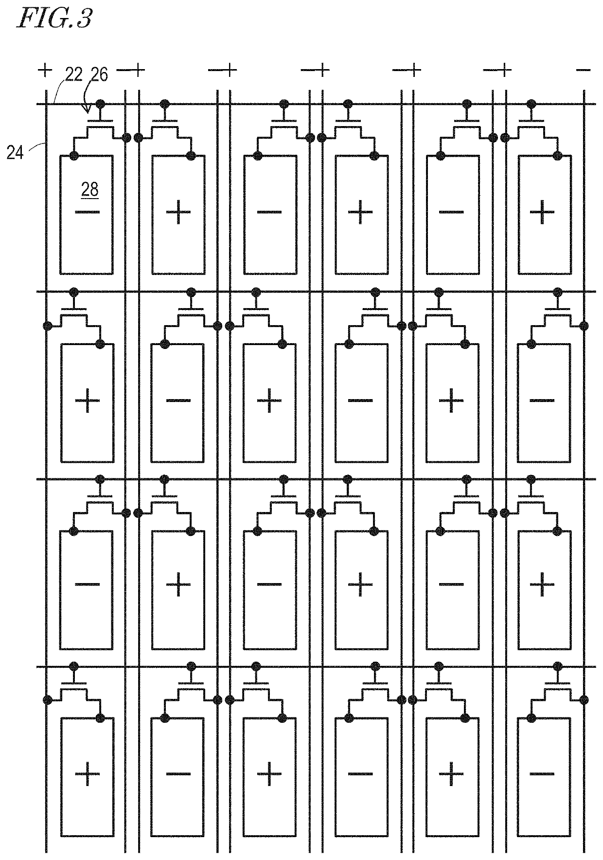
[0001]This application claims priority under 35 USC § 119(e) to U.S. Provisional Application No. 63 / 158,564 filed on Mar. 9, 2021, the entire contents of which are hereby incorporated by reference.BACKGROUND1. Technical Field[0002]The present invention relates to a liquid crystal display apparatus.2. Description of the Related Art[0003]A liquid crystal display apparatus is driven such that the polarity of a voltage applied to a liquid crystal layer in pixels (direction of the electric field generated in the liquid crystal layer) is inverted on a time period-by-time period basis in order to prevent image burn-in (e.g., frame inversion driving). In addition, in order to prevent flicker of an image, a driving method of changing the direction of the electric field on a pixel-by-pixel basis is adopted. For example, a driving method that generates a dot checker pattern or a vertical stripe pattern is known. Herein, the “dot” represents a “pixel”. The “dot checker pattern” is a pattern in ...

Claims


Application Information

Patent Timeline
Patent Type & Authority Applications(United States)
IPC IPC(8): G09G3/36
CPCG09G3/3607G09G3/3614G09G3/3696G09G2330/045G09G2330/021G09G2360/16G09G2300/0426G09G2320/0271G09G2340/16
Inventor YABUKI, HARUHITO
Owner SHARP KK
Learn More