
Flexible Display Device and Method of Manufacturing the Same

Pending Publication Date: 2022-05-12
LG DISPLAY CO LTD
View PDF6 Cites 0 Cited by
  • Summary
  • Abstract
  • Description
  • Claims
  • Application Information

AI Technical Summary

Benefits of technology

This patent describes a way to prevent leakage between pixels in a display made of organic light emitting layers. This is done by using an inverse-tapered structure that can be placed next to a tapered structure. This approach improves the design flexibility of the display, and it allows for a thinner and more flexible device to be created without increasing its thickness. Additionally, the inverse-tapered structure improves adhesion and reduces peeling defects by ensuring both sides of the structure are in contact with a bank.

Problems solved by technology

The continuous application of the tensile stress and the compressive stress due to repeated folding may cause a peeling defect in which multiple layers included in the organic light emitting display device are separated from one another, and this may negatively affect the reliability of the flexible organic light emitting display device.
In particular, an organic light emitting layer among multiple layers included in the organic light emitting display device is the most vulnerable part due to the difficulty of implementing the patterning for relieving folding stress, and relatively weak adhesion.

Method used


Image

  • Flexible Display Device and Method of Manufacturing the Same
  • Flexible Display Device and Method of Manufacturing the Same
  • Flexible Display Device and Method of Manufacturing the Same

Examples


Embodiment Construction

[0024]The advantages and features of the present disclosure and methods of achieving the same will be apparent by referring to embodiments of the present disclosure as described below in detail with reference to the accompanying drawings. It should be noted that the present disclosure is not limited to embodiments set forth below and may be implemented in various different forms. Thus, embodiments of the present disclosure are provided for specifically describing the present disclosure and for specifically informing those skilled in the art to which it pertains of the scope of the present disclosure, and the scope of the present invention is defined only by the scope of the appended claims.

[0025]In addition, the shapes, sizes, ratios, angles, numbers, and the like illustrated in the accompanying drawings for describing the exemplary embodiments of the present disclosure are merely examples, and the present disclosure is not limited thereto. Like reference numerals generally denote l...


PUM


Abstract

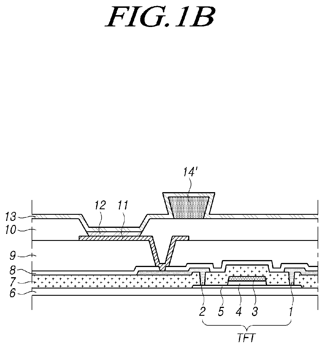
The present disclosure relates to a flexible display device including: a substrate over which a thin film transistor is disposed, an intermediate layer disposed to cover the thin film transistor, a first electrode located on the intermediate layer and connected to the thin film transistor, a bank located on the intermediate layer and the first electrode and defining a first region exposing a part of the intermediate layer, a second region exposing a part of the first electrode, and a third region excluding the first and second regions, a first structure located in the first region defined by the bank and tapered toward the substrate, an organic light emitting layer located on the first electrode exposed in the second region, and a second electrode disposed on the organic light emitting layer. Both lateral surfaces of an inverse-tapered structure are disposed to contact the bank, and as a result, corresponding adhesion can be improved, and peeling defects can be reduced or corrected.

Description

CROSS-REFERENCE TO RELATED APPLICATION[0001]This application claims the priority benefit of Korean Patent Application No. 10-2020-0149102, filed on Nov. 10, 2020 in the Korean Intellectual Property Office, the disclosure of which is incorporated herein by reference in its entirety.BACKGROUNDField of the Disclosure[0002]The present disclosure relates to flexible display devices and method of manufacturing the same, and more specifically, to a flexible display device for minimizing a peeling defect of an organic light emitting layer by including a structure with an inverse taper shape and method of manufacturing the same.Description of the Background[0003]Image display devices configured to display various information or data on a display screen act as a core device in the information and communication era. The display devices become thinner and lighter and are being developed to have high performance while being portable. Among various types of display devices, there are growing need...

Claims


Application Information

Patent Timeline
IPC IPC(8): H01L27/32H01L51/56G09F9/30
CPCH01L27/3246H01L51/56H01L2227/323H01L2251/5338G09F9/301H10K59/12H10K59/122H10K77/111H10K59/1201H10K2102/311H10K50/80H10K59/124H10K71/00
Inventor LEE, KYOUNGMOOK
Owner LG DISPLAY CO LTD
Learn More