Electromagnetic radiation detection structure with optimised absorption and method for forming such a structure
a technology of electromagnetic radiation and structure, applied in the direction of optical radiation measurement, radiation control devices, instruments, etc., can solve the problems of not enabling optimal absorption, the total impedance of the structure, and the inability to achieve optimal absorption, so as to reduce the bias voltage of the gate and therefore the heat released by the transistor during operation, the effect of reducing the bias voltage and reducing the influen
- Summary
- Abstract
- Description
- Claims
- Application Information
AI Technical Summary
Benefits of technology
Problems solved by technology
Method used
Image
Examples
first embodiment
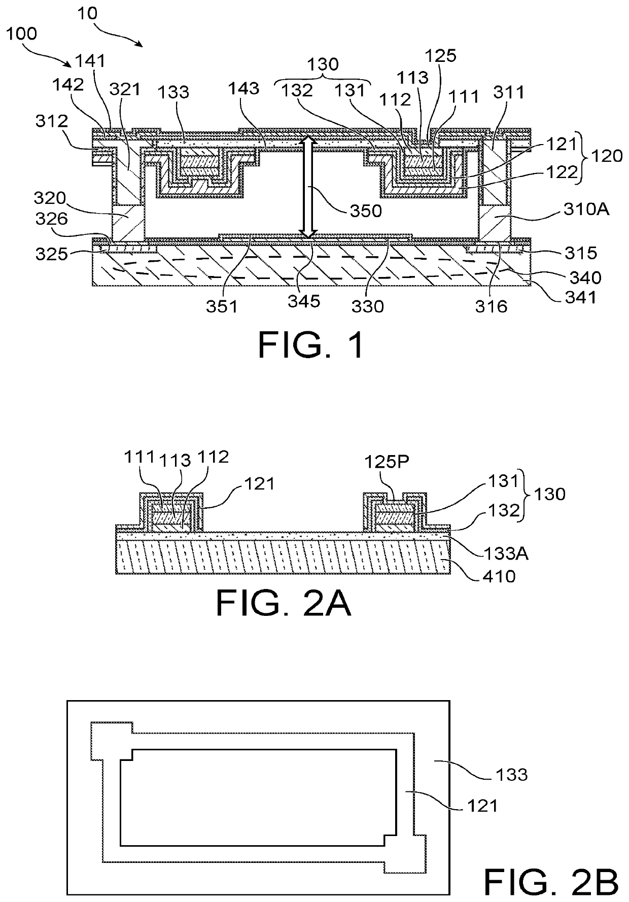
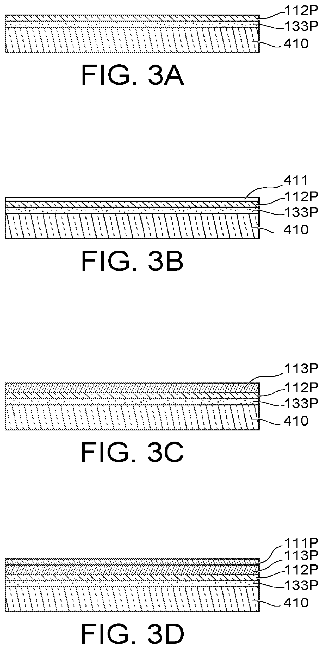
[0090]It will be noted, however, that preferably the stack formed by the first, second and third layers 111P, 112P, 113P is arranged to surround at least partly the zone of the detection structure which is called the detection zone. The parts of the gate electrode 120 and the ohmic contact 125 of the second zone 112 forming the first and second absorbing elements 121 extend at least partly along said detection zone. It will be noted that in this first embodiment only the second absorbing element extends entirely along the detection zone, the first absorbing element 121 having only minority portions extending along the detection zone.
[0091]According to this possibility, the stack formed by the first, second and third zones 111, 112, 113 can, for example, have:[0092]a comb-like configuration, the surrounded absorption zones being the zones disposed between the arms of the comb, or[0093]a serpentine-like configuration, the absorption zones surrounded being the zones defined between the...
third embodiment
[0173]According to the invention, not illustrated, the first conductive layer 121 can extend along the detection zone and define, for the part of the first conductive layer 121 extending along the detection zone, the absorption plane. It will be noted that by “extending along the detection zone” it is meant that the part of the first conductive layer 121 extends parallel to, and near, the detection zone.
[0174]Thus, a detection structure 1 in this third embodiment is differentiated from a detection structure 1 in the first embodiment in that:[0175]it is the first conductive layer 121 which defines, for at least its part extending along the detection zone, the absorption plane, the quarter-wave cavity 350 thus being formed between the first semiconductor layer 121 and the reflective surface 330,[0176]the third conductive layer 125 does not extend along the detection zone.
[0177]A method for manufacturing a detection structure 1 according to this third embodiment is differentiated from ...
PUM
| Property | Measurement | Unit |
|---|---|---|
| total impedance | aaaaa | aaaaa |
| equivalent resistance | aaaaa | aaaaa |
| equivalent resistance | aaaaa | aaaaa |
Abstract
Description
Claims
Application Information
 - R&D
- Intellectual Property
- Life Sciences
- Materials
- Tech Scout
- Unparalleled Data Quality
- Higher Quality Content
- 60% Fewer Hallucinations
Browse by: Latest US Patents, China's latest patents, Technical Efficacy Thesaurus, Application Domain, Technology Topic, Popular Technical Reports.
© 2025 PatSnap. All rights reserved.Legal|Privacy policy|Modern Slavery Act Transparency Statement|Sitemap|About US| Contact US: help@patsnap.com


