Method of manufacturing semiconductor device

Active Publication Date: 2021-09-30
CANON KK
View PDF0 Cites 0 Cited by
  • Summary
  • Abstract
  • Description
  • Claims
  • Application Information

AI Technical Summary

Benefits of technology

The present invention relates to a method for manufacturing semiconductor devices using an exposure apparatus. The method includes a first period for exposing substrates using a first reticle, a second period for exposing substrates using a second retical, and a third period between the first and second periods. The first retical is changed to the second retical during the third period and control is performed to adjust the temperature distribution of the optical element in the projection optical system to reduce aberration during the first and second periods. The technical effect of this patent is that it suppresses changes in aberration of the projection optical system during the use of multiple reticles, which improves the accuracy of the semiconductor device manufacturing process.

Problems solved by technology

Hence, the change in the aberration generated due to the incidence of exposure light in the projection optical system tends to be large immediately after the start of an exposure operation, but will gradually saturate thereafter.
However, as can be understood from the characteristics of the change in the aberration as described above, the change of the aberration of the projection optical system that occurs immediately after the start of the second exposure job can be large if such a method is employed.

Method used


Image

  • Method of manufacturing semiconductor device
  • Method of manufacturing semiconductor device
  • Method of manufacturing semiconductor device

Examples


Embodiment Construction

[0019]Hereinafter, embodiments will be described in detail with reference to the attached drawings. Note, the following embodiments are not intended to limit the scope of the claimed invention. Multiple features are described in the embodiments, but limitation is not made to an invention that requires all such features, and multiple such features may be combined as appropriate.

[0020]Furthermore, in the attached drawings, the same reference numerals are given to the same or similar configurations, and redundant description thereof is omitted.

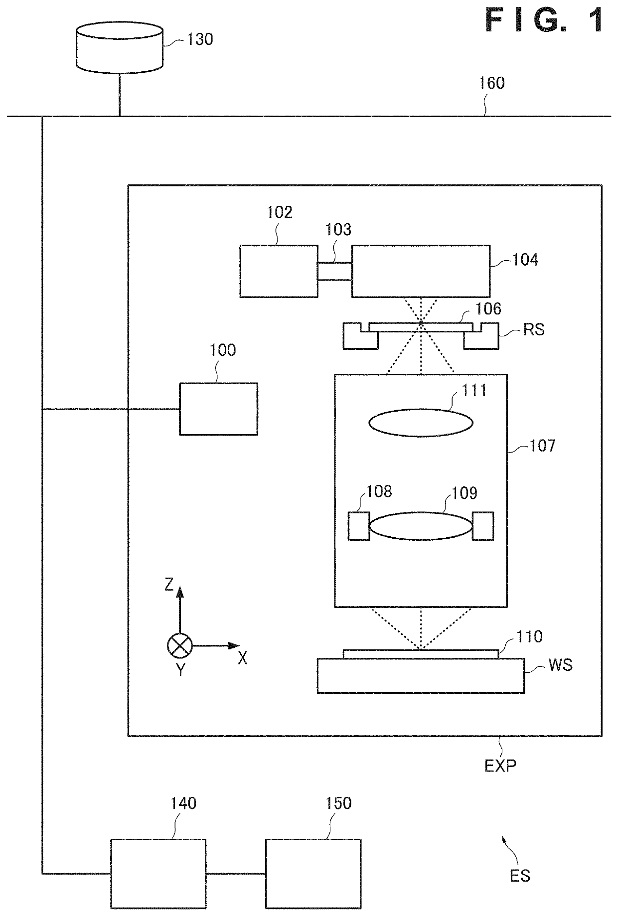
[0021]An embodiment will be described with reference to the accompanying drawings hereinafter. FIG. 1 schematically shows the arrangement of an exposure system ES which includes an exposure apparatus EX. A substrate 110 to which a photoresist has been applied by a resist application apparatus (not shown) is conveyed to the exposure apparatus EXP. The substrate 110 can typically be a wafer made of a semiconductor such as silicon or the like, it ma...


PUM


Abstract

A method of manufacturing a semiconductor device by using an exposure apparatus having a reticle stage and a projection optical system includes a first period in which substrates are exposed by using a first reticle arranged on the reticle stage, a second period in which substrates are exposed by using a second reticle arranged on the reticle stage, and a third period which is between the first and second periods. The method includes changing, in at least part of the third period, the first reticle arranged on the reticle stage to the second reticle, and performing control, in the first and second periods, to adjust temperature distribution of an optical element of the projection optical system so as to reduce change in aberration of the projection optical system. The third period is shorter than the first period.

Description

BACKGROUND OF THE INVENTIONField of the Invention[0001]The present invention relates to a method of manufacturing a semiconductor device.Description of the Related Art[0002]Japanese Patent Laid-Open No. 2006-73584 discloses an exposure apparatus that cancels, in a case in which a non-rotation symmetric aberration that occurs due to incidence of exposure light in a projection optical system has exceeded a tolerance value, the execution of an exposure operation until the non-rotation symmetric aberration becomes equal to or less than the tolerance value.[0003]Note that the characteristics of a change of an aberration generated due to incidence of exposure light in a projection optical system is generally expressed by (1−exp(−Δt / T)). At is an elapsed time from a given time, and T is a time constant. Hence, the change in the aberration generated due to the incidence of exposure light in the projection optical system tends to be large immediately after the start of an exposure operation,...

Claims


Application Information

Patent Timeline
IPC IPC(8): G03F7/20H01L21/027
CPCG03F7/706G03F7/70891H01L21/0274G03F7/70725G03F7/70258G03F7/70733G03F7/70425G03F1/00G03F7/70008G03F7/7055G03F7/70216H01L21/027G03F7/70525
Inventor TOYODA, TAKEHIROKOBAYASHI, HIROAKIINA, HIDEKIASANO, KOSUKEMIYANO, KOUKI
Owner CANON KK
Why Eureka
Try Eureka