Memory scaling semiconductor device

Active Publication Date: 2021-08-12
SANDISK TECH LLC
View PDF5 Cites 0 Cited by
  • Summary
  • Abstract
  • Description
  • Claims
  • Application Information

AI Technical Summary

Benefits of technology

The present technology relates to a memory module that includes two separately accessible electrical units, each containing a memory array and bond pads. The two memory modules are bonded together to avoid warping and chipping of thinner dies, and the overall thickness of the memory module can be reduced to 25 μm or below. The architecture allows for independent management of yield losses related to wafer-to-wafer integration, and ensures no good die is wasted. The integrated memory module also allows for serially connecting the two dies, decoupling of bad dies from the stack, and high-density memory design. The technical effects of this technology include reduced thickness of the memory module, improved mechanical stability, higher memory density, and more efficient use of good dies.

Problems solved by technology

Mechanical factors such as die warping, chipping and / or cracking during semiconductor package fabrication are proving a barrier to further reduction in thickness of semiconductor dies.
For example, heating of the semiconductor dies during package fabrication causes the dies to warp given the different coefficients of thermal expansion between the memory device layers and silicon substrate.
Moreover, when dies are thinned, for example to below 36 μm, die chipping or cracking when handled during fabrication also becomes a significant problem preventing further reductions in the thicknesses of semiconductor dies.

Method used


Image

  • Memory scaling semiconductor device
  • Memory scaling semiconductor device
  • Memory scaling semiconductor device

Examples


Embodiment Construction

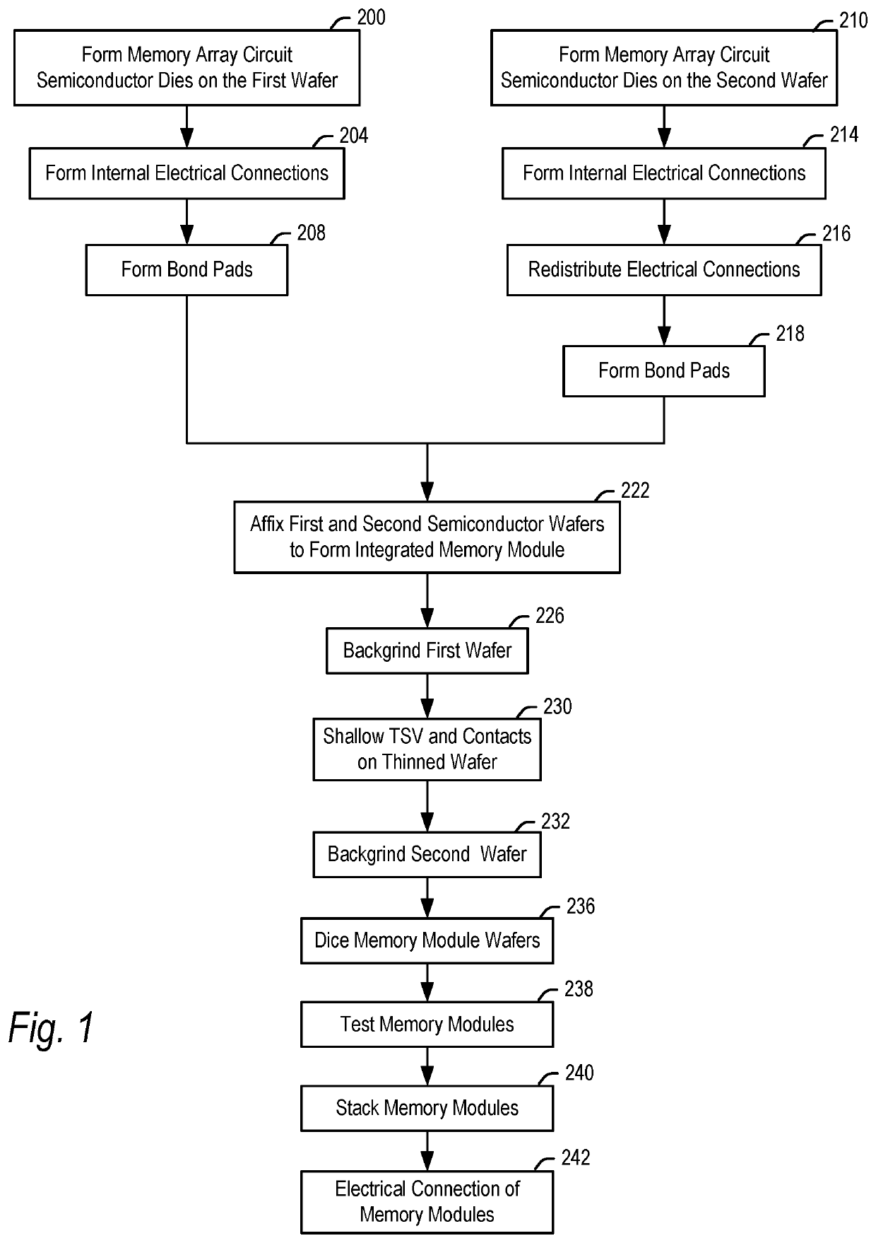
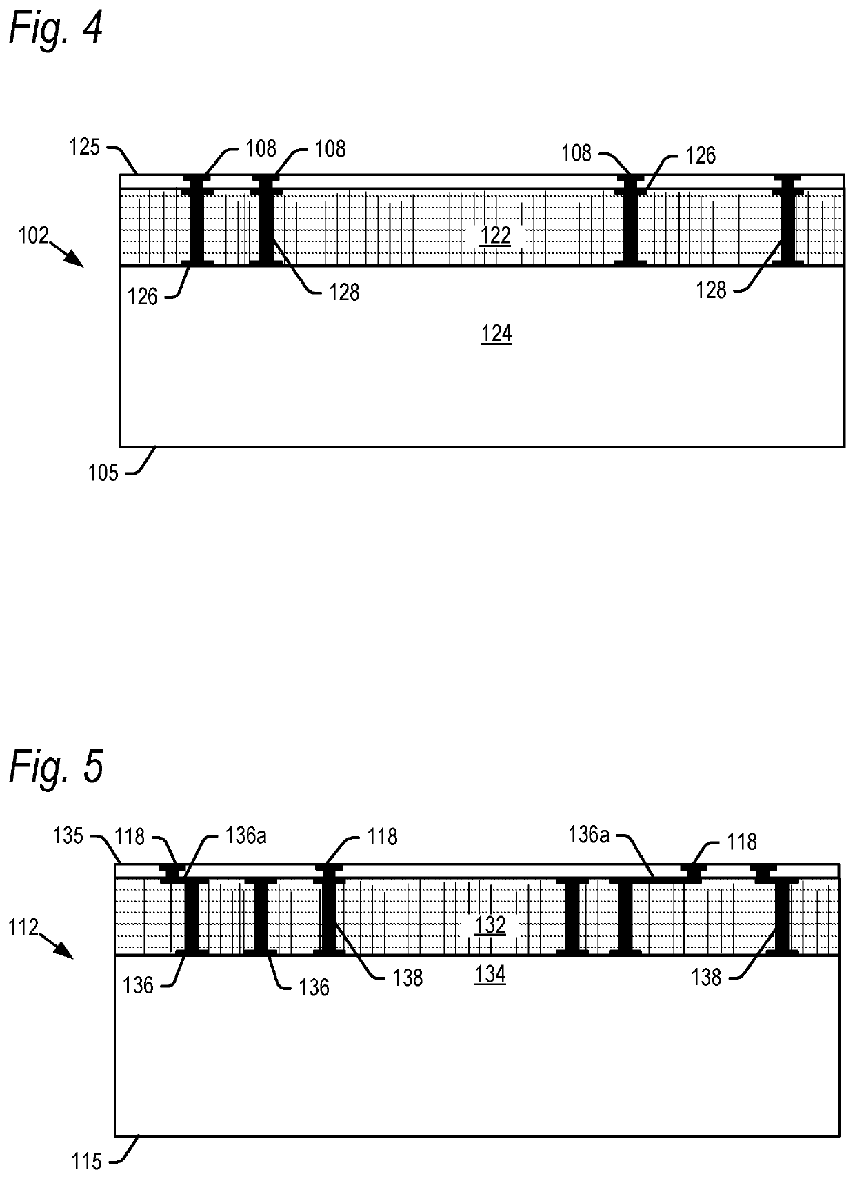
[0030]The present technology will now be described with reference to the figures, which in embodiments, relate to a semiconductor device including an integrated memory module. The integrated memory module may include a pair of semiconductor dies, having a device layer formed in a silicon substrate. The pair of dies may be affixed to each other face to face; that is, with their active surfaces facing each other. In such a configuration, the disparate coefficients of thermal expansion of the device layers and silicon substrate balance each other to prevent warping of the module. This ability to prevent warping in part enables a high memory density device where the thicknesses of the respective dies in the module may be thinner than was previously achievable. Additionally, the overall thickness of the module may be sufficient to avoid chipping or cracking during handling of the module during fabrication.

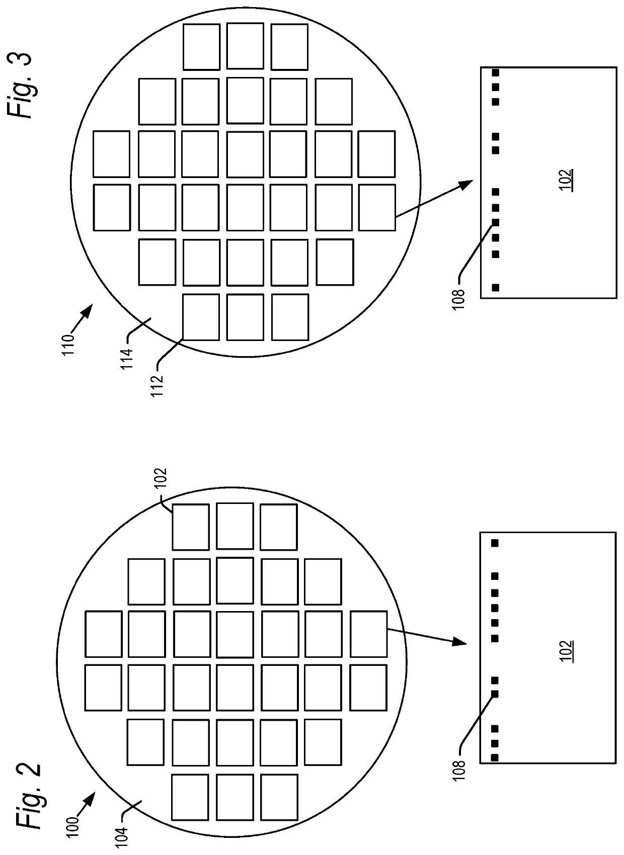
[0031]Economies of scale may be achieved by fabricating a number of memory modules ...


PUM


Abstract

A semiconductor device is disclosed including a memory module formed from a pair of semiconductor dies mounted face to face to each other at the wafer level. These die pairs are formed using wafer-to-wafer bonding technology, where the wafers may be bonded to each other when they are of full thickness. Once bonded, respective inactive surfaces of the wafers may be thinned and then the die pairs diced from the wafers to form a completed memory module. When the wafers are bonded face to face, they compensate each other, mechanically resulting in the die pair having a minimum warpage.

Description

PRIORITY DATA[0001]This application is a divisional of U.S. patent application Ser. No. 16 / 594,716 filed on Oct. 7, 2019 entitled “MEMORY SCALING SEMICONDUCTOR DEVICE”, which application is incorporated herein by reference in its entirety.BACKGROUND[0002]The strong growth in demand for portable consumer electronics is driving the need for high-capacity storage devices. Non-volatile semiconductor memory devices, such as flash memory storage cards, are widely used to meet the ever-growing demands on digital information storage and exchange. Their portability, versatility and rugged design, along with their high reliability and large capacity, have made such memory devices ideal for use in a wide variety of electronic devices, including for example digital cameras, digital music players, video game consoles, PDAs, cellular telephones and solid state drives (SSDs).[0003]Recently, ultra high density memory devices have been proposed using a 3D stacked memory structure having strings of m...

Claims


Application Information

Patent Timeline
IPC IPC(8): H01L25/065H01L23/00H01L25/00
CPCH01L25/0657H01L24/48H01L24/08H01L23/562H01L25/50H01L2225/06506H01L2225/06586H01L2924/3511H01L2225/06562H01L2225/06541H01L2224/08146H01L2225/06524H01L2224/48147H01L2224/08145H01L2224/0557H01L2225/06513H01L2225/06517H01L2225/06565H01L2225/0651H01L2224/0401H01L2224/04042H01L2224/94H01L25/0652H01L2924/15311H01L2924/1815H01L2924/19104H01L25/16H01L27/105H01L24/80H01L2224/80895H01L2224/80896H01L2224/48145H01L2224/80006H01L2224/8001H01L2224/8003H01L2224/80201H01L2224/80099H01L2224/80097H01L2224/95H01L2224/80357H01L2224/80379H01L2224/09181H01L2224/9202H01L2224/85399H01L2224/05647H01L2224/05124H01L2224/45099H01L2224/05147H01L2224/05111H01L2224/05138H01L2224/05144H01L2224/05155H01L2224/8083H01L2224/80H01L2224/80001H01L2224/03H01L2924/00014H01L2924/059H01L2924/04642H01L2924/05042H01L2924/01014H01L2924/013H01L2924/00013H01L2924/05442
Inventor VODRAHALLI, NAGESH
Owner SANDISK TECH LLC
Why Eureka
Try Eureka