Memory device including test control circuit

Active Publication Date: 2021-06-10
SK HYNIX INC
View PDF0 Cites 0 Cited by
  • Summary
  • Abstract
  • Description
  • Claims
  • Application Information

AI Technical Summary

Benefits of technology

[0009]In accordance with an embodiment, a semiconductor memory device can verify defects of various register circuits as well as the memory cell array included therein, using a BIST circuit for a self test operation of the semiconduct

Problems solved by technology

The increase in integration density of semiconductor memory devices raises the possibility that defects will occur in the semiconductor memory devic

Method used


Image

  • Memory device including test control circuit
  • Memory device including test control circuit
  • Memory device including test control circuit

Examples


Embodiment Construction

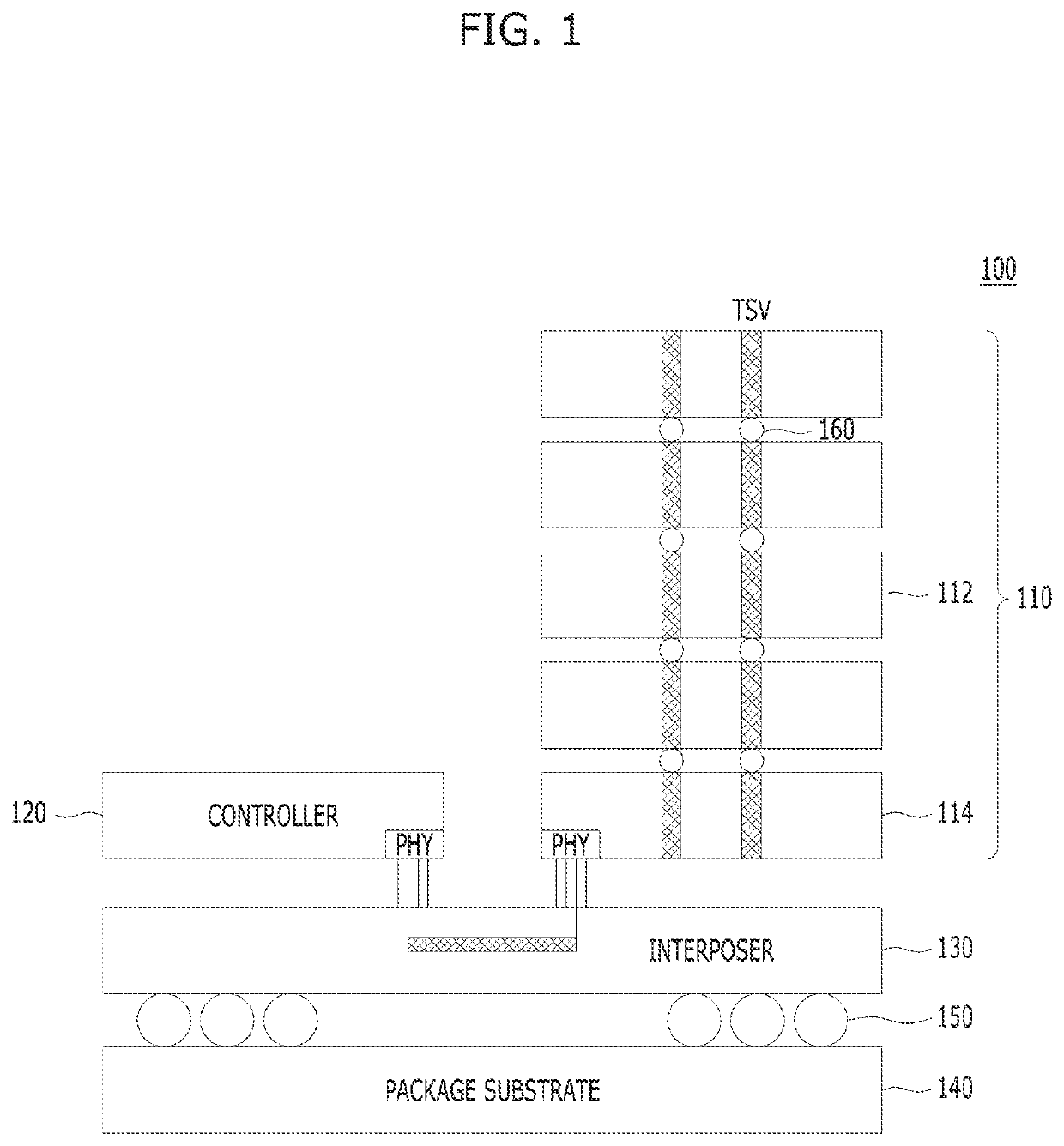
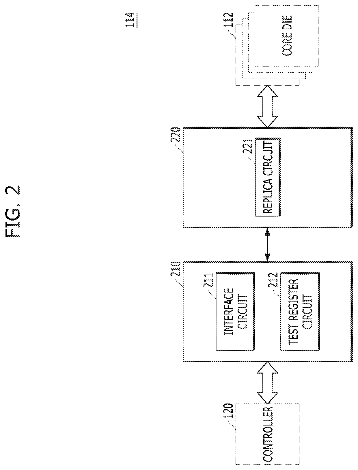
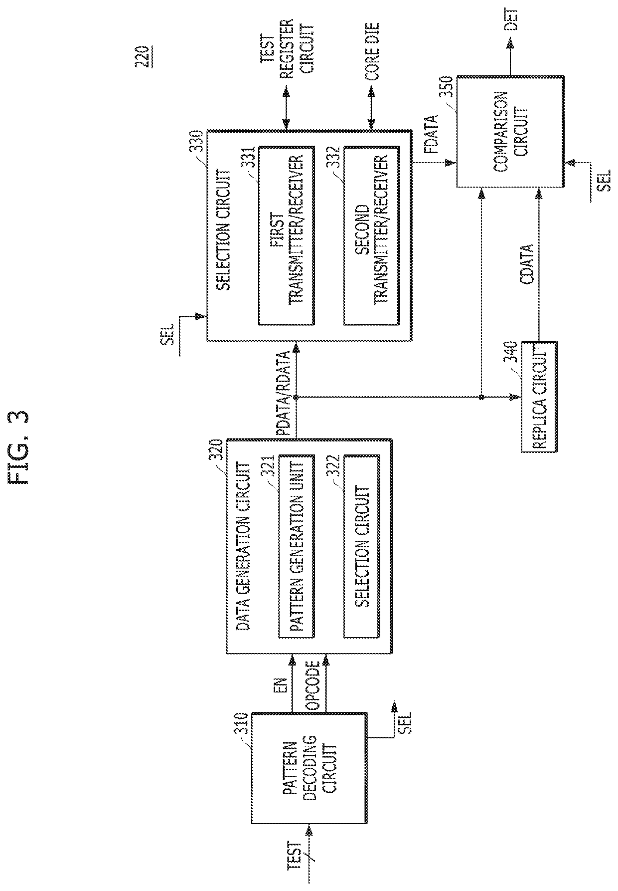
[0014]Various embodiments are described below in detail with reference to the accompanying drawings. The present teachings may, however, be embodied in different forms and should not be construed as being limited to the embodiments set forth herein. Rather, these embodiments are provided so that this disclosure will be enabling, and will convey the scope of the present teachings to those skilled in the art. Throughout the disclosure, like reference numerals refer to like parts throughout the various figures and embodiments of the present teachings.

[0015]Throughout the specification, when one element is referred to as being ‘connected to’ or ‘coupled to’ another element, it may indicate that the former element is directly connected or coupled to the latter element or electrically connected or coupled to the latter element with another element interposed therebetween. Furthermore, when an element “includes” or “comprises” a component, it means that the element does not exclude another...


PUM


Abstract

A memory device includes a memory cell array suitable for storing data, an input/output circuit suitable for inputting and outputting the data stored in the memory cell array, a test register circuit suitable for testing the input/output circuit, and a test control block comprising a replica circuit configured by modeling the test register circuit, and suitable for generating data to test the test register circuit.

Description

CROSS-REFERENCE TO RELATED APPLICATION[0001]This application claims priority under 35 U.S.C. § 119 to Korean Patent Application No. 10-2019-0163684 filed on Dec. 10, 2019, which is incorporated herein by reference in its entirety.BACKGROUND1. Field[0002]Embodiments relate to a memory device having a test control circuit, and more particularly, to a memory device capable of performing a self test operation using a test control circuit therein, and a memory system including the same.2. Discussion of the Related Art[0003]With the demand for high integration and high performance semiconductor memory devices, the technology for packaging a plurality of semiconductor memory chips has continuously developed. Therefore, semiconductor memory devices having a 3D structure instead of a 2D structure are fabricated. The 2D structure is a structure in which a plurality of semiconductor memory chips are horizontally arranged on a PCB (Printed Circuit Board) through wires or bumps, and the 3D struc...

Claims


Application Information

Patent Timeline
IPC IPC(8): G11C29/38G11C29/36
CPCG11C29/38G11C2029/3602G11C29/36G11C29/12G11C29/20G11C29/24G11C29/1201G11C29/022
Inventor JU, YUCHEONCHO, HOSUNG
Owner SK HYNIX INC
Why Eureka
Try Eureka