Fingerprint sensing device
- Summary
- Abstract
- Description
- Claims
- Application Information
AI Technical Summary
Benefits of technology
Problems solved by technology
Method used
Image
Examples
Embodiment Construction
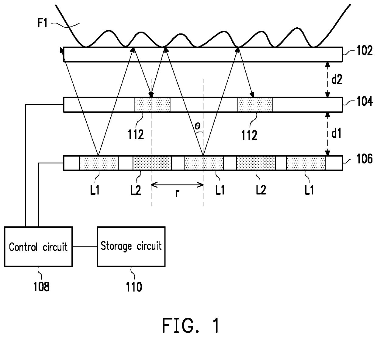
[0011]FIG. 1 is a schematic diagram of a fingerprint sensing device according to an embodiment of the invention. Referring to FIG. 1, the fingerprint sensing device may include a glass cover 102, a sensing layer 104, a light source layer 106, a control circuit 108, and a storage circuit 110, where the control circuit 108 is coupled to the sensing layer 104, the light source layer 106 and the storage circuit 110, and the sensing layer 104 is disposed between the glass cover 102 and the light source layer 106.
[0012]The glass cover 102 may receive a finger F1 of a user when performing fingerprint recognition. The sensing layer 104 includes a plurality of sensing units 112, and the sensing units 112 are configured to sense a fingerprint image of the user, where each of the sensing units 112 may include, for example, at least one light sensor. The storage circuit 110 may store characteristic data of a fingerprint. The light source layer 106 includes a plurality of point light sources, an...
PUM
 Abstract
Description
Claims
Application Information
 - R&D
- Intellectual Property
- Life Sciences
- Materials
- Tech Scout
- Unparalleled Data Quality
- Higher Quality Content
- 60% Fewer Hallucinations
Browse by: Latest US Patents, China's latest patents, Technical Efficacy Thesaurus, Application Domain, Technology Topic, Popular Technical Reports.
© 2025 PatSnap. All rights reserved.Legal|Privacy policy|Modern Slavery Act Transparency Statement|Sitemap|About US| Contact US: help@patsnap.com


