Borophenes, boron layer allotropes and methods of preparation
a technology of boron allotropes and borophenes, which is applied in the direction of boron/borides, etc., can solve the problems of notably sparse experimental investigations of nanostructured boron allotropes
- Summary
- Abstract
- Description
- Claims
- Application Information
AI Technical Summary
Benefits of technology
Problems solved by technology
Method used
Image

Examples
example 1
[0061]Auger Electron Spectroscopy.
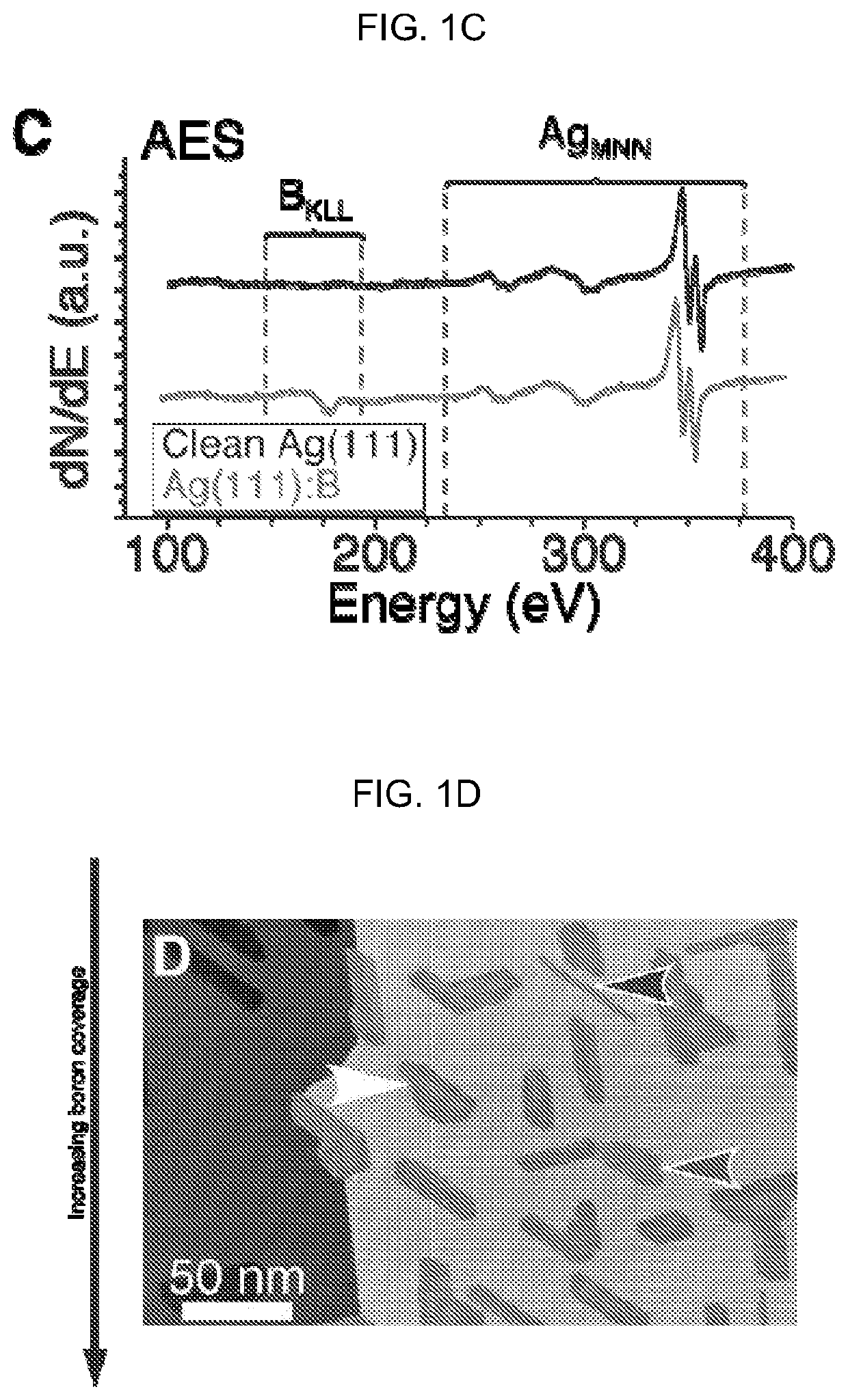
[0062]Auger Electron Spectroscopy (AES) in situ verified the cleanliness of the surface before deposition, and the chemical identity of the samples following STM measurements. Auger transitions respond to changes in the local chemical environment due to shifts in both the valence and core level energies. The formation of compounds generally results in shifts of at least several eV. Low atomic number elements like boron are especially susceptible to these shifts.
[0063]Representative AES spectra obtained on clean Ag(111), Ag(111) with borophene, and Ag(111) with a thicker (−4-6 ML) amorphous boron film are presented in FIG. 5A. In the clean Ag(111) spectrum, the characteristic Ag MNN spectrum is observed, with sharp peaks at 351 and 356 eV and broad secondary peaks at 263 and 303 eV. Boron deposition does not noticeably modify the silver peaks, indicating there was no substantial chemical modification to the surface (i.e., no alloying or compound form...
example 2
[0065]Low Energy Electron Diffraction.
[0066]Spatially averaged atomic structural data is obtained through in situ low-energy electron diffraction (LEED). In LEED, the magnitude of the reciprocal space scattering vector q is given by
|qhk→|=1|Ghk|
where Ghk represents the real-space translation vector of the surface and h and k represent the indices of the diffraction spot. The sampled region of reciprocal space is inversely proportional to the electron de Broglie wavelength; therefore, higher electron energy images larger reciprocal lattice vectors (i.e., smaller real space distances).
[0067]Reciprocal space structural data are also obtained by performing a fast Fourier transform (FFT) on STM images. FIGS. 7A-7B show sequentially acquired topography images of the Ag(111) surface and a nearby region of striped / rectangular phase. FIG. 7C shows the superposition of FFTs on FIGS. 7A-7B, where the spots related to the Ag(111) and boron structures are highlighted in red and blue, respectivel...
example 3
[0069]Structure and Morphology of the Homogeneous Phase.
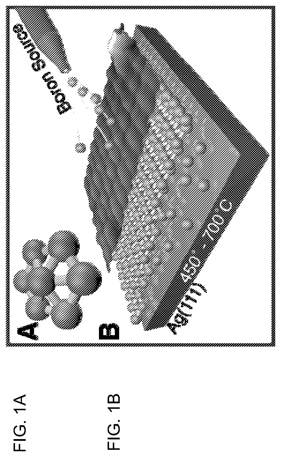
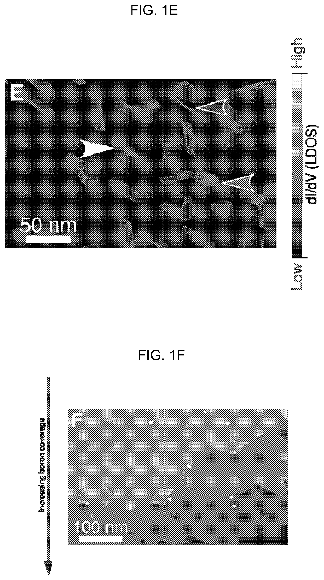
[0070]Several grains of the homogeneous phase are shown in FIGS. 1D-1E. Homogeneous phase islands typically exhibit truncated triangle or truncated oval (i.e., “bullet-like”) shapes. No homogeneous phase islands were observed for growth at 700° C., suggesting that high temperature and / or slow deposition enable the kinetically limited phase transformation from the homogeneous phase to the striped phase to proceed. Although the homogeneous phase islands often appear featureless at the large scale, they exhibit multiple scales of Moire pattern, including a ˜0.9 nm rhombohedral pattern, and one-dimensional Moire patterns with ˜8 nm periodicity, as in FIGS. 8A-8B. The 1D Moire pattern correlates to variations in the degree of lateral distortion of the chain features in the atomic-scale structure (FIG. 8B). Concurrent with this chain structure, bias dependent imaging reveals additional structure connecting adjacent chains (FIG. 8C), ...
PUM
| Property | Measurement | Unit |
|---|---|---|
| temperature | aaaaa | aaaaa |
| temperature | aaaaa | aaaaa |
| temperature | aaaaa | aaaaa |
Abstract
Description
Claims
Application Information
 - R&D
- Intellectual Property
- Life Sciences
- Materials
- Tech Scout
- Unparalleled Data Quality
- Higher Quality Content
- 60% Fewer Hallucinations
Browse by: Latest US Patents, China's latest patents, Technical Efficacy Thesaurus, Application Domain, Technology Topic, Popular Technical Reports.
© 2025 PatSnap. All rights reserved.Legal|Privacy policy|Modern Slavery Act Transparency Statement|Sitemap|About US| Contact US: help@patsnap.com