
Device Structure for a 3-Dimensional NOR Memory Array and Methods for Improved Erase Operations Applied Thereto

Active Publication Date: 2020-02-13
SUNRISE MEMORY CORP
View PDF0 Cites 110 Cited by
  • Summary
  • Abstract
  • Description
  • Claims
  • Application Information

AI Technical Summary

Benefits of technology

The present invention provides a thin-film storage transistor with improved erase efficiency. This is achieved by adding one or more sources of holes in close proximity to the floating P-channel region of the transistor. The transistor includes semiconductor layers, a conductor, and a charge-trapping structure. The charge-trapping structure includes an oxide-nitride-oxide multi-layer with a dopant concentration greater than 1×1010 cm−3. The third semiconductor layer can be dopant-rich or undoped and is preferably depletable. A fourth semiconductor layer in direct or indirect contact with the channel region can provide free charge carriers to speed up device operations. Dopant redistribution can be prevented by using a thin dielectric diffusion barrier film or prolonged high temperature steps. The technical effect is improved erase efficiency of the thin-film storage transistor.

Problems solved by technology

Unlike non-volatile memory transistors fabricated on bulk silicon, non-volatile thin-film memory transistors (e.g., those disclosed in the Related Applications) have floating channels and therefore suffer from a limited supply of donor or acceptor sites.
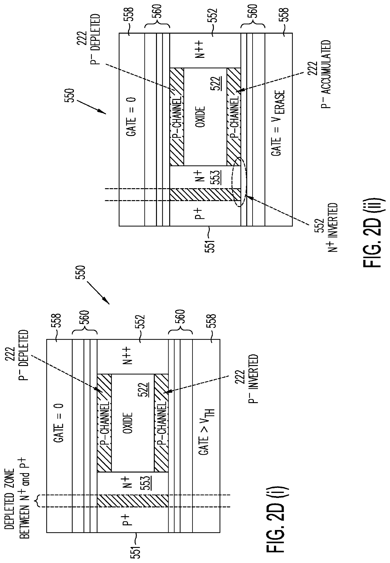
During an erase operation, the gate, source and drain bias conditions of an NMOS thin-film memory transistor may completely deplete the floating channel region of electrons, so that there are insufficient number of holes to accumulate at the surface of the channel region, thereby leading to a slow erase operation.

Method used


Image

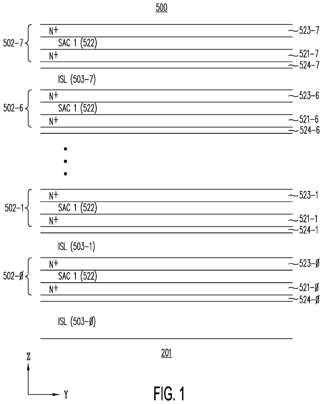
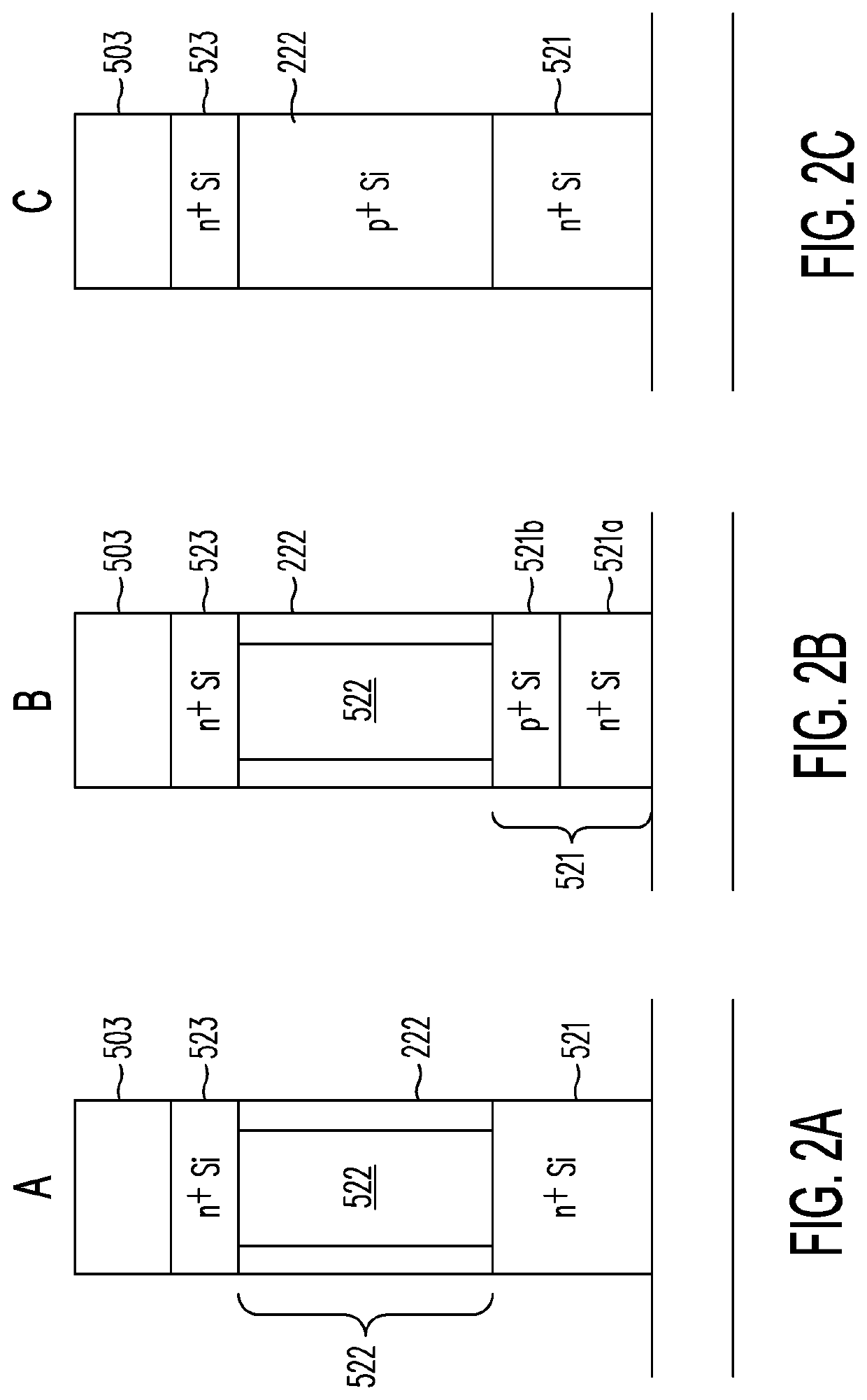
  • Device Structure for a 3-Dimensional NOR Memory Array and Methods for Improved Erase Operations Applied Thereto
  • Device Structure for a 3-Dimensional NOR Memory Array and Methods for Improved Erase Operations Applied Thereto
  • Device Structure for a 3-Dimensional NOR Memory Array and Methods for Improved Erase Operations Applied Thereto

Examples


Embodiment Construction

[0022]The present invention provides one or more sources of holes in close proximity to a floating P− channel in a thin-film storage transistor in order to facilitate a more efficient erase operation. One way to supply excess holes to a channel region to facilitate erase is by generating holes using the well-known GIDL mechanism1. Although it is a relatively slow mechanism (typically a few milliseconds), GIDL is employed extensively in 3-D NAND memory structures to generate holes in the channel region during an erase operation. GIDL bias conditions can be employed equally well to generate excess holes during an erase operation for the thin-film transistors disclosed in the Related Applications. The GIDL mechanism can be applied whether erasing an entire thin-film transistor string or individually selected thin-film transistors. 1 GIDL is the acronym for “gate-induced drain leakage current.”

[0023]Another way to facilitate an erase operation is to connect the P− channel regions of the...


PUM


Abstract

A thin-film storage transistor includes (a) first and second polysilicon layers of a first conductivity serving, respectively, as a source terminal and a drain terminal of the thin-film storage transistor; (b) a third polysilicon layer of a second conductivity adjacent the first and second polysilicon layers, serving as a channel region of the thin-film storage transistor; (c) a conductor serving as a gate terminal of the thin-film storage transistor; and (d) a charge-trapping region between the conductor and third polysilicon layer, wherein a fourth body layer polysilicon of the second conductivity is included to provide an alternative source of free charge careers to accelerate device operation.

Description

CROSS REFERENCE TO RELATED APPLICATIONS[0001]The present application is related to and claims priority of U.S. provisional patent application (“Provisional Application I”), Ser. No. 62 / 697,060, entitled “Device Structure for a 3-Dimensional NOR Memory Array and Methods for Improved Erase Operations Applied Thereto,” filed on Jul. 12, 2018.[0002]The present application relates to (i) U.S. provisional patent application (“Provisional Application II”), Ser. No. 62 / 522,666, entitled “Replacement Metal and Strut for 3D Memory Array”, filed on Jun. 20, 2017; and (ii) U.S. provisional patent application (“Provisional Application III”), Ser. No. 62 / 550,553, entitled “3-Dimensional NOR Memory Array Architecture and Methods for Fabrication Thereof,” filed on Aug. 25, 2017. (iii) U.S. patent application (“Non-provisional Application I”), Ser. No. 15 / 846,766, entitled “Multi-gate NOR Flash Thin-film Transistor Strings Arranged in Stacked Horizontal Active Strips with Vertical Control Gates,” fi...

Claims


Application Information

Patent Timeline
IPC IPC(8): H01L27/11556H01L27/11582G11C16/04G11C11/56H01L27/06H01L27/12
CPCH01L27/0688G11C11/5635H01L27/1214H01L27/11582G11C16/0416H01L27/11556G11C16/0466H01L21/8221H01L29/78642H10B43/27G11C16/0483H10B41/27H10B20/40
Inventor HARARI, ELICERNEA, RAUL ADRIANSAMACHISA, GEORGECHIEN, WU-YI HENRY
Owner SUNRISE MEMORY CORP
Learn More