Integrated circuit system and packaging method therefor

a circuit system and integrated circuit technology, applied in the field of electronic devices, can solve the problems of affecting the mechanical reliability of the chip system, high production cost, and variety of thermomechanical stress problems at the interfaces of different materials, so as to reduce the cost of fabricating a large-plane circuit board, reduce production costs, and avoid warpage of large-sized substrates

Active Publication Date: 2020-01-02
SHENZHEN XIUYUAN ELECTRONICS TECH CO LTD
View PDF3 Cites 1 Cited by
  • Summary
  • Abstract
  • Description
  • Claims
  • Application Information

AI Technical Summary

Benefits of technology

[0051]13. The area of the substrate is greater than 10,000 square centimeters. According to the integrated circuit system package structure and method of the present disclosure, a large-plane circuit board may be fabricated to avoid warpage, ensuring the performance of a large-plane circuit board, and at the same time reducing the cost of fabricating a large-plane circuit board. A large-sized substrate composed of a first device set, a second device set, and a molding material can be fabricated, and at the same time, warpage of the large-sized substrate can be avoided simultaneously, ensuring quality and possibility of continuing the subsequent processes on the large substrate and reducing production costs.
[0052]14. The first device set or / and the second device set includes an invalid device, and the invalid device is used to make uniform the density of the devices of the first device set or / and the second device set are distributed at two sides of the molding material to avoid warpage of the molding material. The device composition of the first device set and the second device set is often determined by the function to be implemented, and the size, dimension, and number may vary greatly. If only valid devices are used, different thermo-mechanical stresses may be present at two sides of the formed substrate due to uneven device material distribution and there may be warpage during the fabrication process. As needed, the invalid device may be set separately in the first device set, or the invalid device may be separately set in the second device set, or the invalid device may be set in both the first device set and the second device set. In the present disclosure, in addition to setting the first device set and the second device set to realize the circuit function of the whole system, an invalid chip is further added, and the invalid chip can offset the difference in volume and occupied area between different devices, enabling uniform device occupied density of the entire molding material surface, further reducing the warpage, reducing the difficulty of the fabrication process, and improving the fabrication precision of the connecting circuit layer. Especially for large-size substrates, the use of invalid devices can greatly reduce the possible warpage of large-sized substrates during the fabrication process.
[0053]15. The first device set and the second device set are staggered at two sides of the molding material, so that the density that the devices of the first device set and the second device set are distributed at the two sides of the molding material is uniform, thereby avoiding warpage of the molding material. The device sets are staggered on the surface of the molding material to avoid possible warpage of the formed large-sized substrate during the fabrication process. The device composition of the first device set and the second device set is often depended on the function to be implemented, and the size, dimension and number may vary greatly. If only valid devices are used, the number of device sets placed increases as the size of the formed substrate increases. If only the same device set is placed on the same side of the substrate, different thermo-mechanical stresses at two sides of the formed substrate caused by the uneven distribution of the device materials is increased accordingly, and during the fabrication process, the warpage of the substrate will also increase. In the present disclosure, the first device set and the second device set may be arranged in a staggered way on the first carrier and the second carrier, so that the device density at the two sides of the finally formed substrate is more uniform, the stresses at the two sides of the substrate after detachment of the first carrier and the second carrier is more symmetrical, and the warpage is less likely to occur. The warpage of the formed large-sized substrate during the fabrication process can be reduced, the difficulty of the fabrication process can be reduced, and the fabrication precision of the connecting circuit layer can be improved.

Problems solved by technology

Since it is often required to be connected to the circuit port of the substrate by wire bonding or flip-chipping, and then connected to the circuit board, the amount of used materials are large, the process is complicated, and the production cost is high; moreover, using a large number of materials with different characteristics may also easily induce a variety of thermomechanical stress problems at the interfaces of the different materials.
During the curing process of an encapsulation layer, due to the large difference in thermal expansion coefficients of various materials, a large thermal stress is generated at the junction of the chip and the substrate, which affects the mechanical reliability of the chip system.
In the newer fan-out system packaging technology, because the chips of multiple systems need to be processed simultaneously on a large-sized panel, during the curing process of the encapsulation layer, warpage of the panel may be easily caused due to difference in the thermal expansion coefficients of the encapsulation layer material, the chip material and the substrate material, seriously affecting the yield of the process and limiting the line width accuracy that can be achieved.
Because of the large difference in thermo-mechanical properties between the device material silicon and the molding material, after being cured and detached from the carrier, the substrate will have large warpage, which seriously affects the implementation of the subsequent processes.
Since the electrical connection is consolidated before the molding material is cured, drifting of the relative position of the chip during the curing process can be avoided, resulting in a huge difficulty in electrical connection of the circuit layer.
If only valid devices are used, different thermo-mechanical stresses may be present at two sides of the formed substrate due to uneven device material distribution and there may be warpage during the fabrication process.
If only the same device set is placed on the same side of the substrate, different thermo-mechanical stresses at two sides of the formed substrate caused by the uneven distribution of the device materials is increased accordingly, and during the fabrication process, the warpage of the substrate will also increase.

Method used


Image

  • Integrated circuit system and packaging method therefor
  • Integrated circuit system and packaging method therefor
  • Integrated circuit system and packaging method therefor

Examples


Embodiment Construction

[0064]The present disclosure will be further described in detail below, but embodiments of the disclosure are not limited thereto.

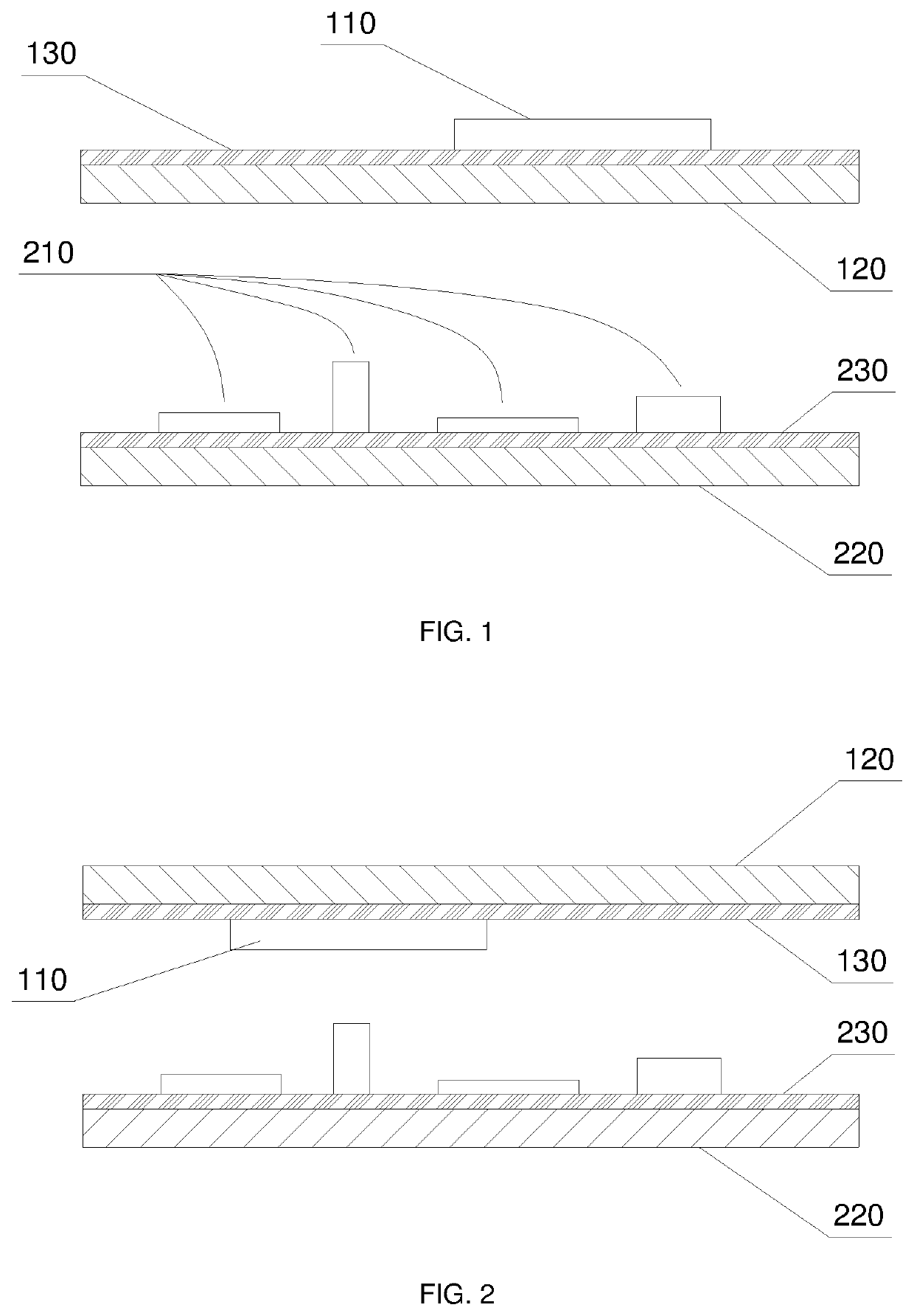
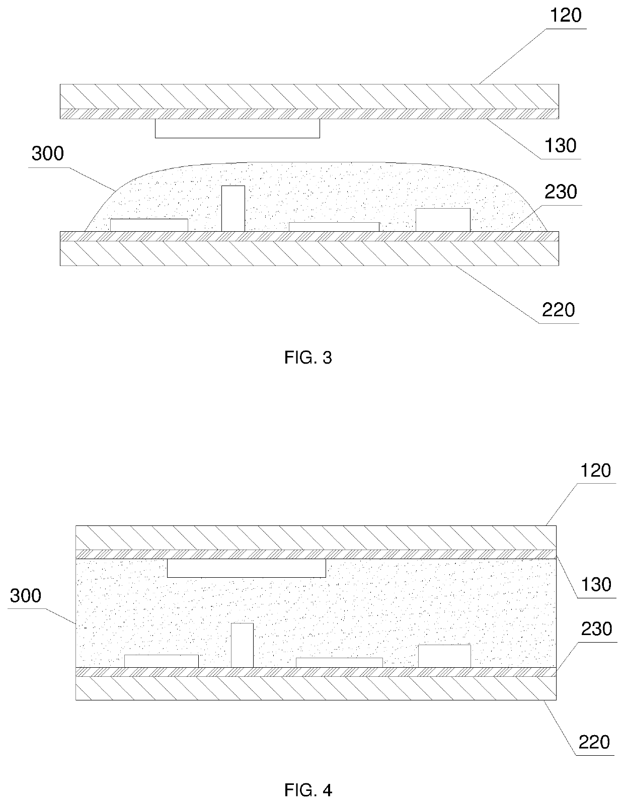
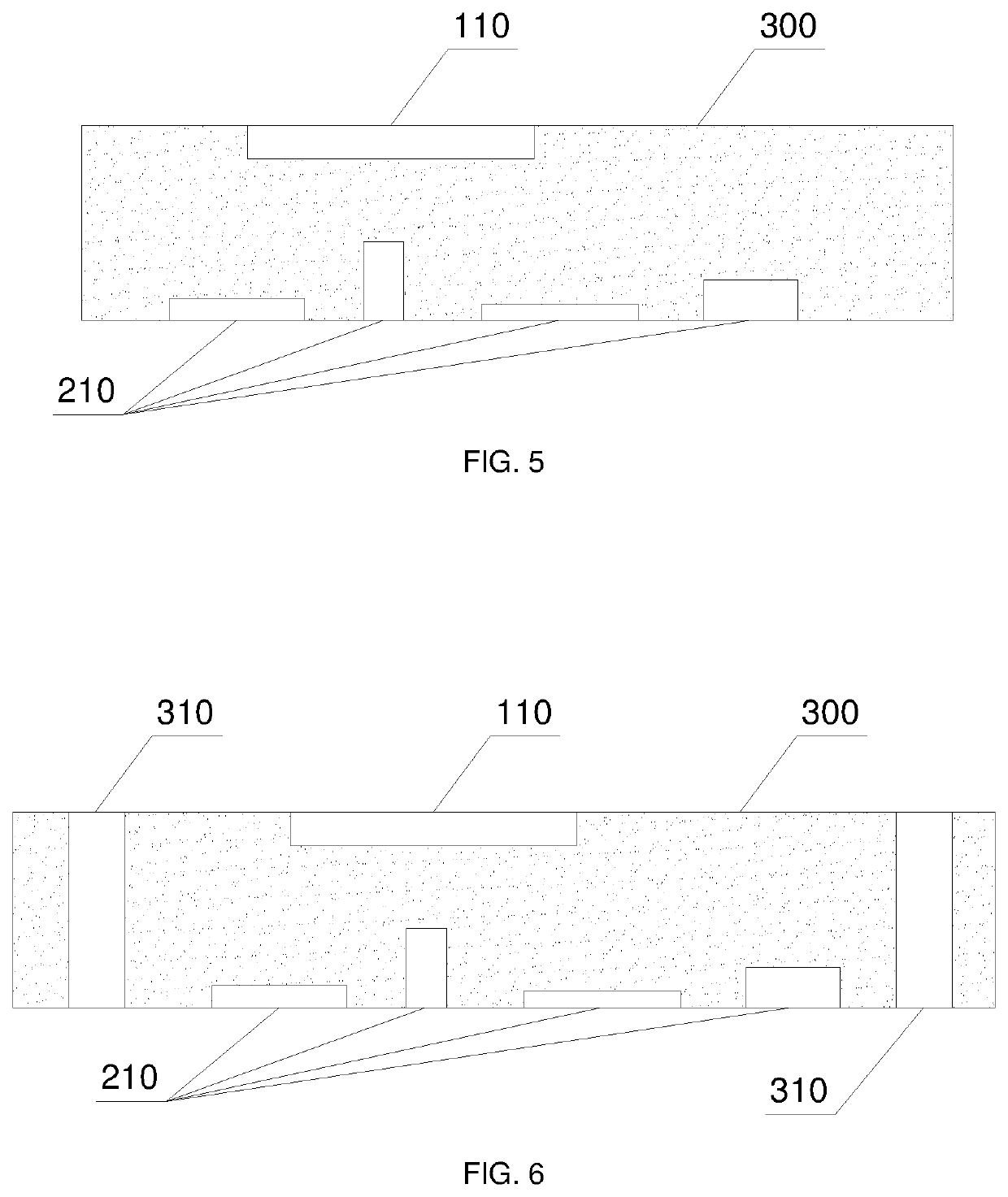
[0065]The integrated circuit system includes: a first device set 110 detached from a first carrier 120, a second device set 210 detached from a second carrier 220, and a cured molding material 300 as shown in FIGS. 1 to 6, wherein the molding material 300 is located between the first device set 110 and the second device set 210, the first device set 110 and the second device set 210 are in contact with the molding material 300, and the first device set 110 and the second device set 210 are respectively mounted at two sides of the molding material 300, the molding material 300 is provided with connection holes 310 and a conductive layer 400, the conductive layer 400 extends into the connection holes 310, and the conductive layer 400 enables the first device set 110 to be electrically connected with the second device set 210. The conductive layer 400 extend...


PUM


Abstract

An integrated circuit system and a packaging method therefor are disclosed. The method includes providing a first carrier and a second carrier oppositely, with a first device set of the first carrier and a second device set of the second carrier both located between the first and second carriers, providing a molding material between the first and second carriers to make the first and second device sets respectively in contact with the molding material, curing the material to make the first and second device sets respectively mounted at two sides of the molding material, making the first and second carriers detached from the first device set and the molding material and from the second device set and the molding material respectively; and forming connection holes in the molding material and fabricating a conductive layer which extend into the connection holes to electrically connect the first and second device sets.

Description

TECHNICAL FIELD[0001]The disclosure belongs to the field of electronics, and in particular relates to an integrated circuit system and a packaging method.BACKGROUND ART[0002]The conventional multi-component or multi-chip system packaging are typically packaging in system units. A plurality of electronic components or chips, which constitutes a system, are flip-chipped or wire-bonded onto one surface or one side of a substrate containing circuits thereinside, and then encapsulated in a molded plastic, which is then soldered or plugged into a circuit board together with other required electronic components or chips, to form a fully-functional integrated circuit system. Since it is often required to be connected to the circuit port of the substrate by wire bonding or flip-chipping, and then connected to the circuit board, the amount of used materials are large, the process is complicated, and the production cost is high; moreover, using a large number of materials with different charac...

Claims


Application Information

Patent Timeline
Patent Type & Authority Applications(United States)
IPC IPC(8): H01L25/00H01L25/18H01L25/16H01L23/498H01L21/56H01L23/31
CPCH01L25/18H01L21/568H01L25/50H01L21/565H01L23/49805H01L23/3185H01L25/162H01L23/552H01L24/24H01L24/82H01L24/96H01L25/10H01L2224/04105H01L2224/24137H01L2224/96H01L2924/181H01L2924/00012
Inventor HU, CHUANLIU, JUNJUNGUO, YUEJINPRACK, EDWARD RUDOLPH
Owner SHENZHEN XIUYUAN ELECTRONICS TECH CO LTD
Why Eureka
Try Eureka