
Image Pixel, Image Acquisition Device, Fingerprint Acquisition Apparatus, and Display Apparatus

a fingerprint acquisition and image acquisition technology, applied in the field of image acquisition technologies, can solve the problems of inability to meet the requirements of manufacturers, thick image acquisition apparatus is usually very thick,

Inactive Publication Date: 2019-06-06
VKANSEE (BEIJING) TECHNOLOGY CO LTD
View PDF6 Cites 9 Cited by
  • Summary
  • Abstract
  • Description
  • Claims
  • Application Information

AI Technical Summary

Benefits of technology

The patent describes an imaging pixel that uses a transparent layer and a microlens to confine the incident light path, resulting in a narrow field of view and a smaller angle of view. This allows for image acquisition without the need for a lens system or a pinhole imaging system, making the device thinner and clearer. A light blocking wall is also included to prevent signal crosstalk between adjacent imaging pixels. Overall, this technology allows for improved image quality in a thinner and clearer device.

Problems solved by technology

Because a structure such as a lens system is used, an existing image acquisition apparatus is usually very thick.
However, as electronic devices are trending to be required to be ultra-thin, a thick image acquisition apparatus cannot meet the requirement of manufacturers.

Method used


Image

  • Image Pixel, Image Acquisition Device, Fingerprint Acquisition Apparatus, and Display Apparatus
  • Image Pixel, Image Acquisition Device, Fingerprint Acquisition Apparatus, and Display Apparatus
  • Image Pixel, Image Acquisition Device, Fingerprint Acquisition Apparatus, and Display Apparatus

Examples


Embodiment Construction

[0040]Exemplary embodiments of the present invention will be described below in more detail with reference to the accompanying drawings for the embodiments so that the technical solutions in accordance with the embodiments of the present invention are more clear and complete. Apparently, the described embodiments are merely some rather than all of the embodiments of the present invention. All other embodiments achieved by persons of ordinary skill in the art based on the embodiments of the present application without creative efforts shall fall within the protection scope of the present application.

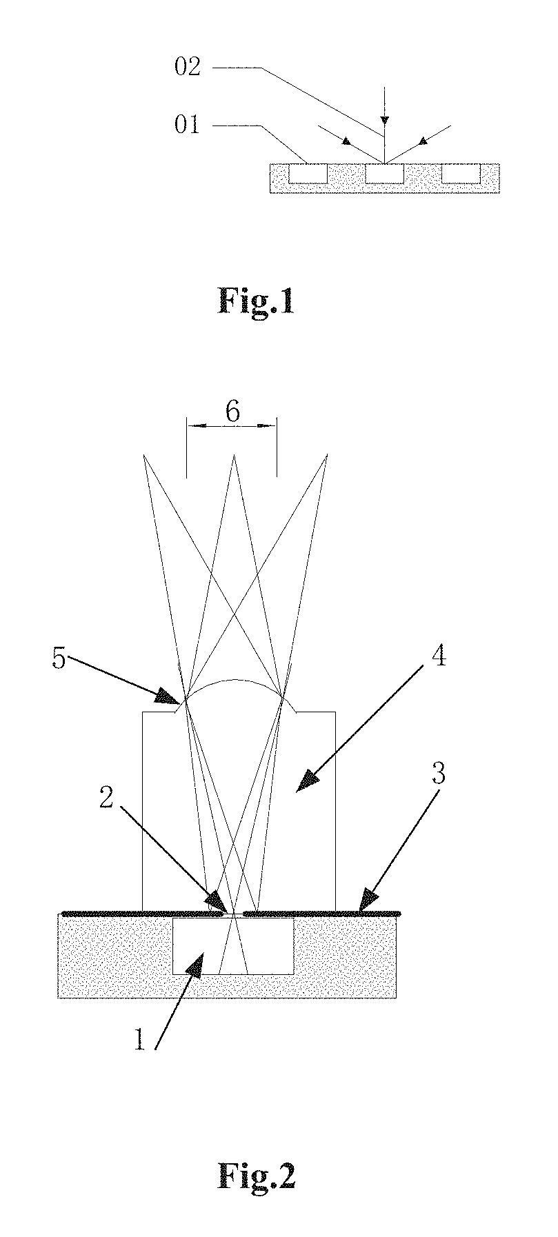
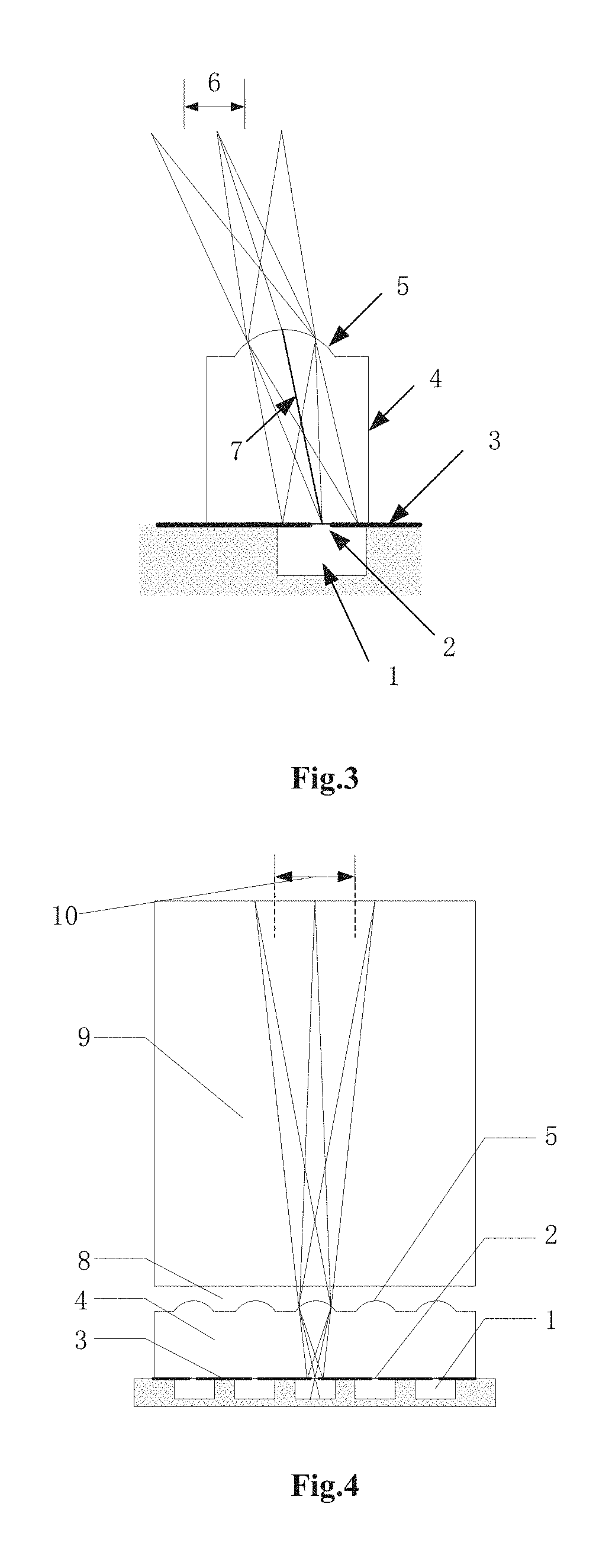
[0041]FIG. 2 is a schematic structural diagram illustrating an imaging pixel according to a preferred embodiment. As shown in FIG. 2, the imaging pixel includes a cavity 1 in which an optical-to-electrical conversion unit is accommodated. A light blocking film 3 with a light transmission pinhole 2 covers over the cavity 1. A transparent medium layer 4 and a microlens 5 are sequentially di...


PUM


Abstract

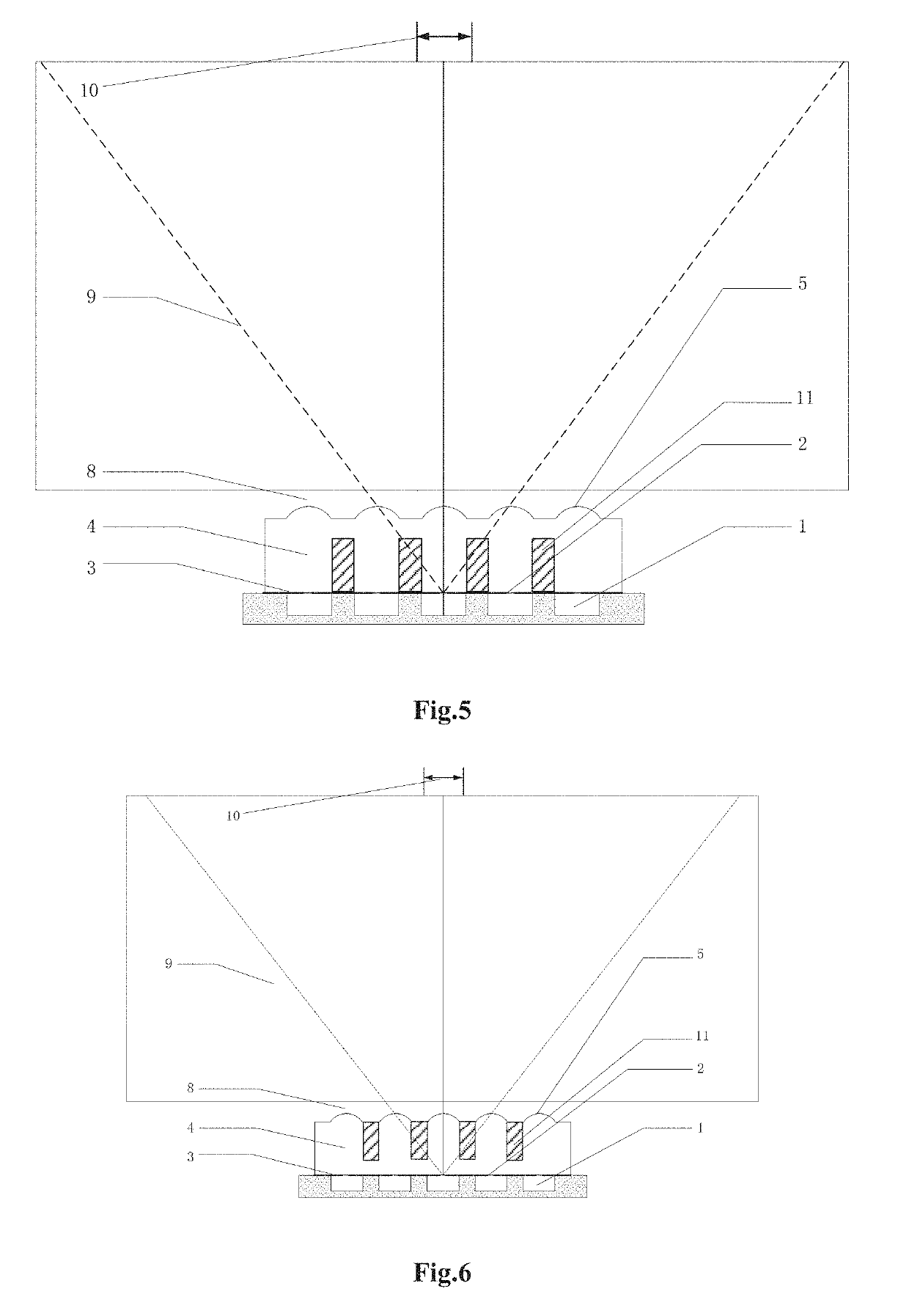
Disclosed are an imaging pixel, an image acquisition device, a fingerprint acquisition apparatus, and a display apparatus supporting an acquisition function. The imaging pixel includes a cavity (1) in which an optical-to-electrical conversion unit is accommodated. A light blocking film (3) with a light transmission pinhole (2) covers over the cavity (1), and a transparent medium layer (4) and a microlens (5) are sequentially disposed on the light blocking film (3) from bottom to top. The microlens (5), the transparent medium layer (4), and the light transmission pinhole (2) are provided so that the imaging pixel has an object-side field of view (6) with a confined angle of view. An image point or an image spot of an object point within the object-side field (6) of view falls within the light transmission pinhole (2) of the light blocking film (3); and an image point or an image spot of an object point outside the object-side field (6) of view falls outside the light transmission pinhole (2). The pinhole on the light blocking film and the microlens confine an incident light path, so that the imaging pixel has a narrow field of view. An image acquisition device based on the imaging pixel with the narrow field of view can confine an incident light path without a lens system or a pinhole imaging system, so that it becomes possible that the image acquisition device can become thinner so as to integrate with another device while acquiring a clear image.

Description

[0001]The present application claims priority of Chinese Patent Application No. 201610357410.0, filed with the Chinese Patent Office on May 25, 2016 and entitled “IMAGING PIXEL, IMAGE ACQUISITION DEVICE, FINGERPRINT ACQUISITION APPARATUS, AND DISPLAY APPARATUS”, which is incorporated herein by reference in its entirety.TECHNICAL FIELD[0002]The present application relates to the field of image acquisition technologies, and specifically to an imaging pixel with a narrow angle of view, an image acquisition device using the imaging pixel, and an optical fingerprint acquisition apparatus.BACKGROUND OF THE INVENTION[0003]In an image acquisition device, a minimum unit for receiving an optical signal is an imaging pixel, and the image acquisition device is usually provided with several imaging pixels. Imaging pixels used in commercially available image acquisition devices all have a wide angle of view. An angle of view of an imaging pixel refers to a maximum angle formed by incident light r...

Claims


Application Information

Patent Timeline
IPC IPC(8): G06K9/00G06F3/042A61B5/1172G06V40/13
CPCG06K9/00026G06F3/0421A61B5/1172G06V40/1324G06V40/13G02B3/0037G06V40/1318G06V40/1335
Inventor ZHANG, MINGFANGNIU, XINGYU
Owner VKANSEE (BEIJING) TECHNOLOGY CO LTD
Learn More