
Camera module and molded photosensitive assembly and manufacturing method therefor, and electronic device

Active Publication Date: 2019-05-30
NINGBO SUNNY OPOTECH CO LTD
View PDF4 Cites 21 Cited by
  • Summary
  • Abstract
  • Description
  • Claims
  • Application Information

AI Technical Summary

Benefits of technology

The patent describes a camera module and its molded photosensitive assembly. The technical effects of the invention include avoiding damage to the wire and electronic components, preventing contamination or damage to the photosensitive area, and ensuring imaging quality and yield during packaging. Another advantage is that the supporting member is made of elastic material and can absorb impact force generated during the molding process. The supporting member is either formed from an elastic material or an inflexible material with a covering film to prevent gaps and damage to the photosensitive area.

Problems solved by technology

Therefore, the size of the camera module can not be effectively reduced in the COB packaging process and the packaging efficiency of the camera module is relatively low.
And limited by the bonding process and the properties of the wire, after the two ends of the wire are soldered to the photosensitive element and the wire board, the wire is curved upwardly and protruded from the upper surface of the photosensitive element.
Once the wire is deformed, the wire is difficult to return to its original shape when the upper mold is removed.
The ability to transmit electrical signals between the photosensitive element and the circuit board of the deformed wire is greatly reduced, so that the imaging capability and imaging efficiency of the camera module are adversely affected.
More importantly, when the wire is deformed by the pressing surface of the upper mold, the deformation direction and degree of deformation of the wire are uncontrollable.
Therefore, two adjacent deformed wires may come in contact with each other that would cause a short-circuit, which leads to increasing the defect rate of the camera module.
In addition, after the photosensitive element is mounted on the circuit board, a gap is formed between the photosensitive element and the circuit board.
Once the mounting relationship between the photosensitive element and the circuit board is changed, it inevitably causes inclination between the photosensitive element and the circuit board which adversely affects the imaging quality of the camera module.

Method used


Image

  • Camera module and molded photosensitive assembly and manufacturing method therefor, and electronic device
  • Camera module and molded photosensitive assembly and manufacturing method therefor, and electronic device
  • Camera module and molded photosensitive assembly and manufacturing method therefor, and electronic device

Examples


Embodiment Construction

[0367]The following description is disclosed to enable any person skilled in the art to make and use the present invention. Preferred embodiments are provided in the following description only as examples and modifications will be apparent to one skilled in the art. The general principles defined in the following description would be applied to other embodiments, alternatives, modifications, equivalents, and applications without departing from the spirit and scope of the present invention.

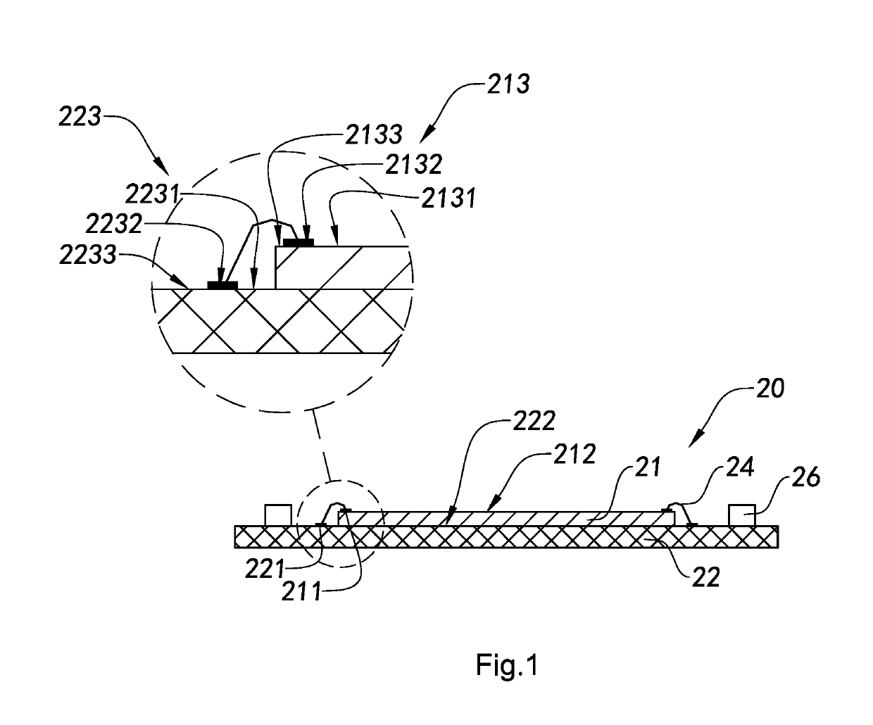
[0368]According to FIGS. 1 to 7 of the drawings of the present invention, a camera module according to a preferred embodiment of the present invention is illustrated, wherein the camera module comprises at least one optical lens 10 and at least one molded photosensitive assembly 20. The at least one molded photosensitive element 20 further comprises a photosensitive element 21, a circuit board 22, a molded base 23, and a set of wires 24, wherein each of the wires 24 has two ends extended to be conn...


PUM


Abstract

A molded photosensitive assembly of a camera module includes at least one supporting member formed by a first substance, at least one photosensitive element, at least one circuit board, at least one set of wires electrically connecting the photosensitive element to the circuit board, and at least one molded base. Two ends of each of the wires are respectively connected to a chip connector of the photosensitive element and a circuit connector of the circuit board. The molded base is formed by a second substance and comprises a molded body and has at least one light window, wherein the photosensitive element and the wires are protected by a supporting member which is provided for avoiding an upper mold of a molding-die pressing on the wires during the molding process.

Description

CROSS REFERENCE OF RELATED APPLICATION[0001]This is a U.S. National Stage under 35 U.S.C. 371 of the International Application Number PCT / CN2016 / 103247, filed Oct. 25, 2016, which claims priority to Chinese application number 201610183447.6, filed Mar. 28, 2016, Chinese application number 201620246631.6, filed Mar. 28, 2016, Chinese application number 201610278035.0, filed Apr. 28, 2016, Chinese application number 201620373323.X, filed Apr. 28, 2016, Chinese application number 201610668807.1, filed Aug. 12, 2016, Chinese application number 201620875383.1, filed Aug. 12, 2016, Chinese application number 201620875381.2, filed Aug. 12, 2016, Chinese application number 201610669214.7, filed Aug. 12, 2016, Chinese application number 201620876056.8, filed Aug. 12, 2016, and Chinese application number 201620875781.3, filed Aug. 12, 2016.BACKGROUND OF THE PRESENT INVENTIONField of Invention[0002]The present invention relates to optical imaging, and more particularly to a camera module and i...

Claims


Application Information

Patent Timeline
IPC IPC(8): H01L27/146H04N5/225H01L23/00
CPCH01L27/14618H04N5/2253H04N5/2257H01L27/14627H01L27/14634H01L27/14636H01L27/14685H01L27/1469H01L24/48H01L23/562H01L2224/48227H01L24/45H01L2224/45139H01L2224/45144H01L2224/45147H04N23/54H01L2924/00014H05K3/0023H04N23/50H05K1/181H01L23/28G03F7/0002H04N23/00H04N23/57
Inventor WANG, MINGZHUCHEN, ZHENYUGUO, NANZHAO, BOJIETANAKA, TAKEHIKOHUANG, ZHENLUAN, ZHONGYUJIANG, HENG
Owner NINGBO SUNNY OPOTECH CO LTD
Learn More