
Method for producing optical component, method for producing product including touch sensor, optical component, and touch sensor device

a technology of optical components and production methods, applied in the direction of instruments, other domestic articles, coatings, etc., can solve the problems of reducing the visual quality affecting the uniformity of the surface of the optical component, and low production efficiency

Active Publication Date: 2019-05-23
JAPAN AVIATION ELECTRONICS IND LTD
View PDF0 Cites 1 Cited by
  • Summary
  • Abstract
  • Description
  • Claims
  • Application Information

AI Technical Summary

Benefits of technology

The invention is about an optical component made of a laminate that includes a film, an adhesive layer, and a substrate. The laminate has flush end surfaces, which improves production efficiency. However, the exposed cut surface of the adhesive layer can cause issues during handling and assembly of the optical component. The invention solves this problem by preventing small pieces of the adhesive layer from peeling off or causing defects while still maintaining the efficiency of the laminate. This allows for the successful assembly of a touch sensor device or other products that include the optical component.

Problems solved by technology

However, in an optical component composed of a laminate formed by bonding a transparent substrate and a transparent film to each other with a layer of an adhesive interposed therebetween like the optical component composed of the laminate of the three-layer structure described in Literature 1, it is not easy but troublesome to accurately align and bond the three layers together so that the laminate has flush end surfaces, resulting in low production efficiency.
However, a peripheral edge of a substrate surface partially does not have the film, which impairs uniformity of the surface of an optical component and reduces visual quality of the optical component.

Method used


Image

  • Method for producing optical component, method for producing product including touch sensor, optical component, and touch sensor device
  • Method for producing optical component, method for producing product including touch sensor, optical component, and touch sensor device
  • Method for producing optical component, method for producing product including touch sensor, optical component, and touch sensor device

Examples


Embodiment Construction

[0025]Embodiments of the present invention will now be described.

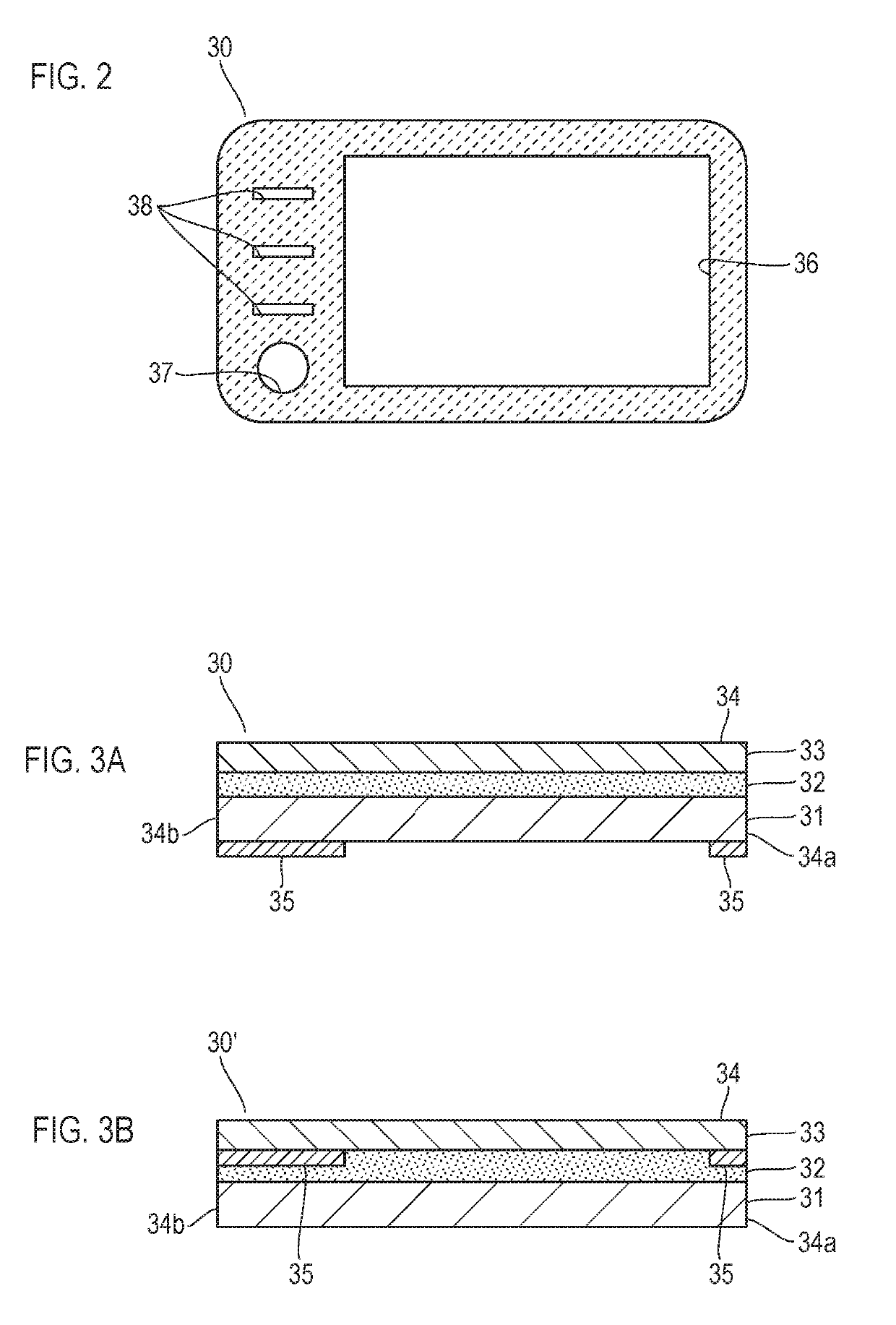
[0026]FIG. 2 shows a brief appearance of a cover provided on a contact input surface of a touch sensor as an embodiment of an optical component of the present invention. FIG. 3A shows a cross-sectional structure thereof. In FIG. 3A, thicknesses of components of the cover are exaggerated.

[0027]A cover 30 is composed of a laminate 34 including a transparent substrate 31, a transparent adhesive layer 32, and a transparent film 33 stacked in this order, and further includes a light blocking design part 35 in this example. In this example, the design part 35 is formed on a peripheral edge of a surface of the substrate 31 opposite to a surface facing the film 33. In FIG. 2, a portion with the design part 35 is hatched, and the contact input surface of the touch sensor is positioned in a transparent region 36 within the frame-like design part 35. In FIG. 2, reference numerals 37, 38 denote holes extending through the cover 30...


PUM

PropertyMeasurementUnit
Temperatureaaaaaaaaaa
Pressureaaaaaaaaaa
Transparencyaaaaaaaaaa

Abstract

A method for producing an at least partially transparent optical component including a laminate including fabricating a precursor laminate by bonding a transparent substrate and a transparent film to each other with a transparent photocurable adhesive layer interposed therebetween; curing the transparent photocurable adhesive layer by applying light thereto to change the precursor laminate into the laminate thereby, such that a shear modulus G′ of the transparent photocurable adhesive layer of the laminate measured under a condition of a temperature of 25° C. and a frequency of 1 Hz reaches a value within a range of 3×10⁵ Pa≤G′≤3×10⁷ Pa; and forming a flush and surface of the laminate by cutting the laminate in a thickness direction, such that the flush end surface includes respective cut surfaces of the transparent film, the transparent photocurable adhesive layer, and the transparent substrate.

Description

TECHNICAL FIELD[0001]The present invention relates to an optical component used as a cover provided on, for example, a contact input surface of a touch sensor and a method for producing the optical component, and also relates to a touch sensor device and a method for producing a product including a touch sensor.BACKGROUND ART[0002]FIG. 1 shows a cross sectional structure of a portable electronic device described in Japanese Patent Application Laid Open No. 2014-160473 (published on Sep. 4, 2014, hereinafter referred to as Literature 1) as an example of a configuration including such the optical component. The portable electronic device includes a casing 11, an insert plate 12, a conductive cushion 13, a touch panel controller 14, a backlight 15, a liquid crystal display part 16, a touch panel part 17, a cover glass 18, an antiscattering film 19, an adhesive 20, a shield ground 21, and a battery 22.[0003]In the configuration in FIG. 1, the cover glass 18 protects the touch panel part...

Claims


Application Information

Patent Timeline
IPC IPC(8): B29D11/00B32B37/12
CPCB29D11/0073B32B37/1284B29D11/00865B29D11/00788B32B2457/20G06F3/041G06F2203/04103C09J5/00C09J133/00C09J2301/312C09J2301/416
Inventor TAKATA, SHINGOKOGAWA, YUTAROITO, EMIKO
Owner JAPAN AVIATION ELECTRONICS IND LTD
Learn More