Method for improving transmittance of flat or curved liquid crystal display panel

Active Publication Date: 2018-08-02
TCL CHINA STAR OPTOELECTRONICS TECH CO LTD
View PDF0 Cites 1 Cited by
  • Summary
  • Abstract
  • Description
  • Claims
  • Application Information

AI Technical Summary

Benefits of technology

The present disclosure provides a method for improving the transparency of flat or curved liquid crystal display panels. This method allows the BPS technology to be compatible with the UV2A technology, resulting in better liquid crystal display transparency. The method involves exposing theCF substrate to light using a mask, and then translating the mask by half the distance of one pixel to start exposing a new domain. The technical effect of this method is improved liquid crystal display transparency.

Problems solved by technology

However, a BPS design is not compatible with the UV2A (Ultraviolet Vertical Alignment) technology, the reason of which is briefly explained below.
Thus, no pattern can be tracked and exposed as the UV2A technology requires.
Therefore, the BPS technology is not compatible with the UV2A technology, due to which it is unlikely to benefit from advantages of the two technologies simultaneously.

Method used


Image

  • Method for improving transmittance of flat or curved liquid crystal display panel
  • Method for improving transmittance of flat or curved liquid crystal display panel
  • Method for improving transmittance of flat or curved liquid crystal display panel

Examples


Embodiment Construction

[0038]The present disclosure will be illustrated further with reference to the drawings.

[0039]The present disclosure provides a method for improving transmittance of flat or curved liquid crystal display panel. The method mainly comprises the following steps.

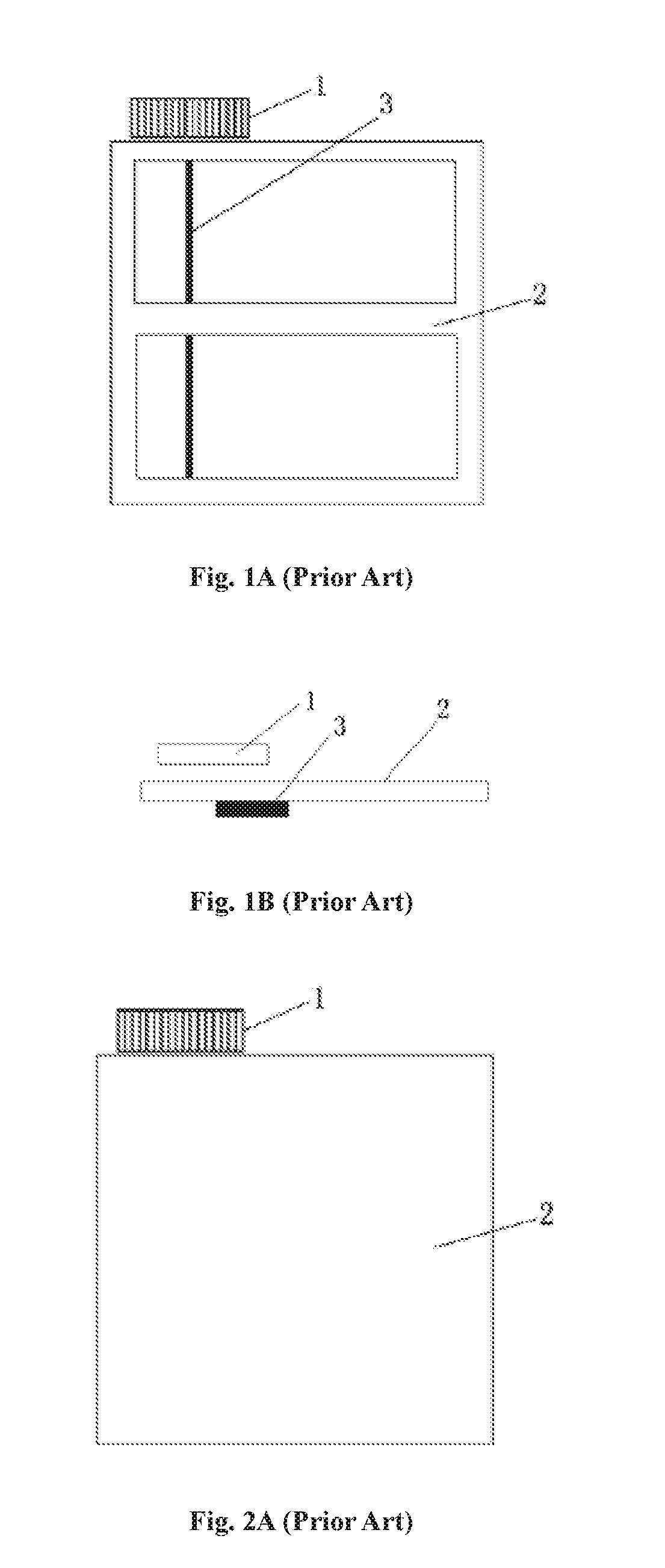
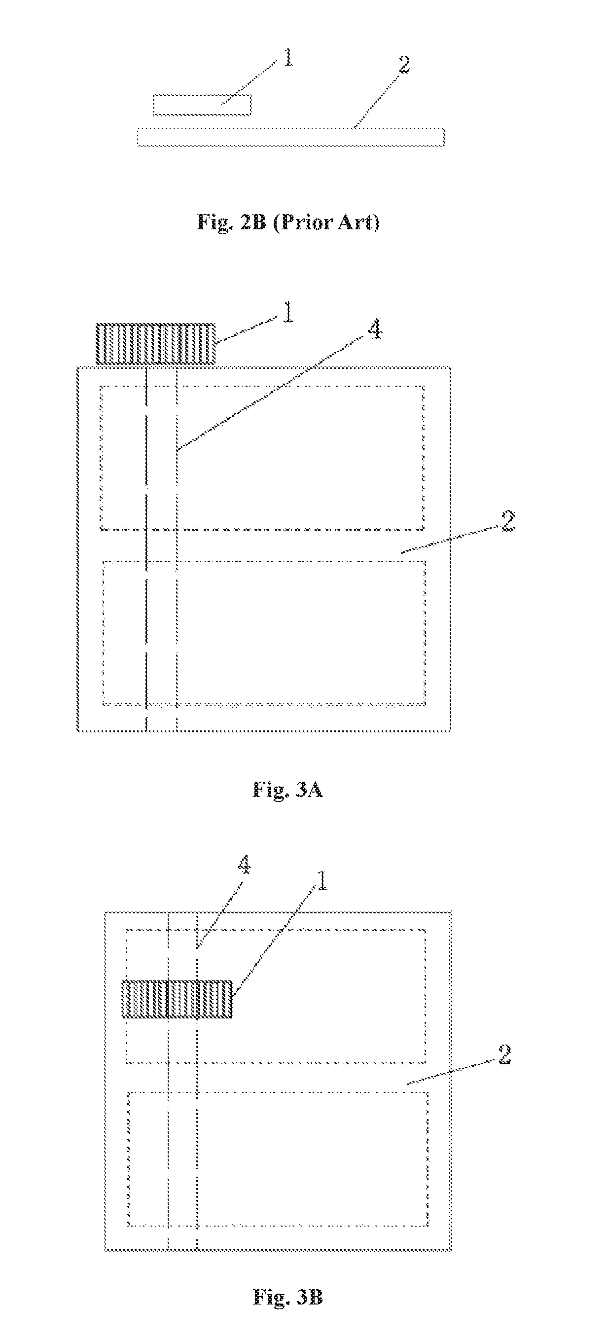
[0040](1) A substrate is manufactured according to the BPS technology. A PS and a BM of the substrate are provided on a side of an array substrate. A transparent conductive electrode (ITO or IZO) film is provided on a side of a CF substrate, which, to be noted, is a technical feature of the BPS technology.

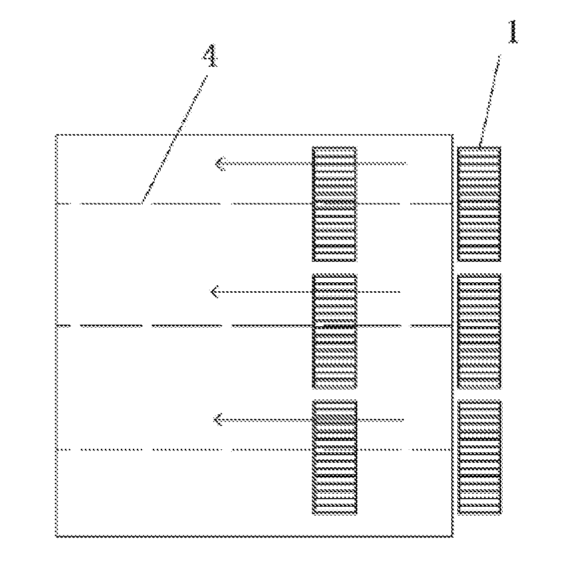
[0041](2) Marks are engraved on designated positions of the CF substrate by means of a laser. In addition to an active area, the marks can also be engraved on positions near edges of the substrate. The CF substrate is aligned with the marks on a platform of a UV2A exposure machine, so as to realize precise alignment. A cell process is then performed. It shall be noted that engraving marks can enable the CF substrate to be preci...


PUM


Abstract

Disclosed is a method for improving transmittance of flat or curved liquid crystal display panel. The method includes the following steps. (1) A substrate is manufactured according to the BPS technology. The substrate includes an array substrate and a CF substrate. A spacer and a black matrix are provided on a side of the array substrate and a transparent conductive electrode film is provided on a side of the CF substrate. (2) Marks are engraved on designated positions of the CF substrate by means of a laser and the CF substrate is aligned with the marks on a platform of a UV2A exposure machine. (3) Tracking lines are engraved on the transparent conductive electrode film and a region bounded by the tracking lines is aligned with a light-shielding region of a gate line or a light-shielding region of a data line on the side of the array substrate. (4) The substrate is exposed to light and a mask is used to track the tracking lines. The method, by taking advantage of a laser patterning method, overcomes the technical prejudices and enables the BPS technology to be compatible with the UV2A technology. Besides, a satisfactory transmittance can also be obtained through the method.

Description

CROSS-REFERENCE TO RELATED APPLICATIONS[0001]The present application claims the priority of Chinese patent application CN 201611258212.5, entitled “Method for improving transmittance of flat or curved liquid crystal display panel” and filed on Dec. 30, 2016, the entirety of which is incorporated herein by reference.FIELD OF THE INVENTION[0002]The present disclosure relates to the technical field of liquid crystal manufacturing, and in particular, to a method for improving transmittance of flat or curved liquid crystal display panel.BACKGROUND OF THE INVENTION[0003]As the liquid crystal display technology develops, a curved surface screen has been invented. For consideration of a curved surface design, a BPS (Black Photo Spacer) design is usually adopted to omit the manufacturing process of a BM (Black Matrix), because a BPS not only has a supporting function like a PS (Photo Spacer), but also can shield a frame area from light, i.e. a BM and a PS are manufactured in one process. Bes...

Claims


Application Information

Patent Timeline
IPC IPC(8): G02F1/1335G02F1/1337G02F1/1333G02F1/1362
CPCG02F1/133512G02F1/133753G02F1/133377G02F1/136209G02F1/133788G02F1/13394G02F1/133354G02F1/13398
Inventor SONG, YANJUNLI, XIANGHSIEH, CHUNG CHINGCHIU, CHUNG YI
Owner TCL CHINA STAR OPTOELECTRONICS TECH CO LTD
Why Eureka
Try Eureka