Display device

Pending Publication Date: 2022-03-10
SAMSUNG DISPLAY CO LTD
View PDF4 Cites 0 Cited by
  • Summary
  • Abstract
  • Description
  • Claims
  • Application Information

AI Technical Summary

Benefits of technology

This patent is about a display device that has good image contrast and transmittance, and minimizes the reflection of external light. The device includes a substrate, a transistor, an interlayer insulating layer, driving and data lines, a passivation layer, a pixel electrode, a pixel defining layer, a light emitting element layer, and a common electrode. The interlayer insulating layer has a groove where the driving and data lines are located. The technical effects of this design are that it prevents external light from being reflected and provides a satisfactory image display quality.

Problems solved by technology

Typically, external light incident on an OLED display device may be reflected on one or more internal surfaces of the OLED display device, undesirably reducing contrast of displayed images.
As a result, the image display quality of the OLED display device may be unsatisfactory.

Method used


Image

  • Display device
  • Display device
  • Display device

Examples


Embodiment Construction

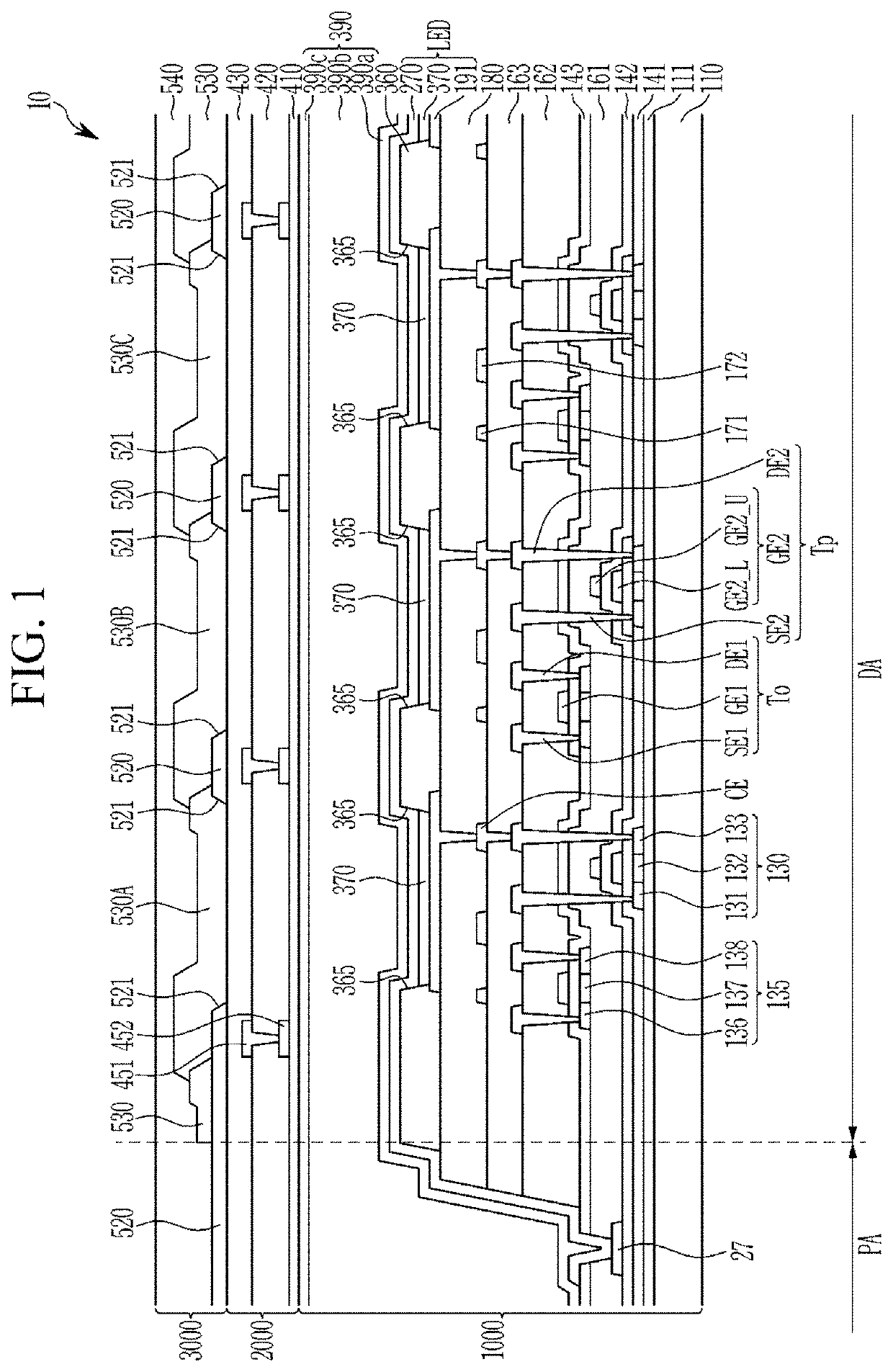
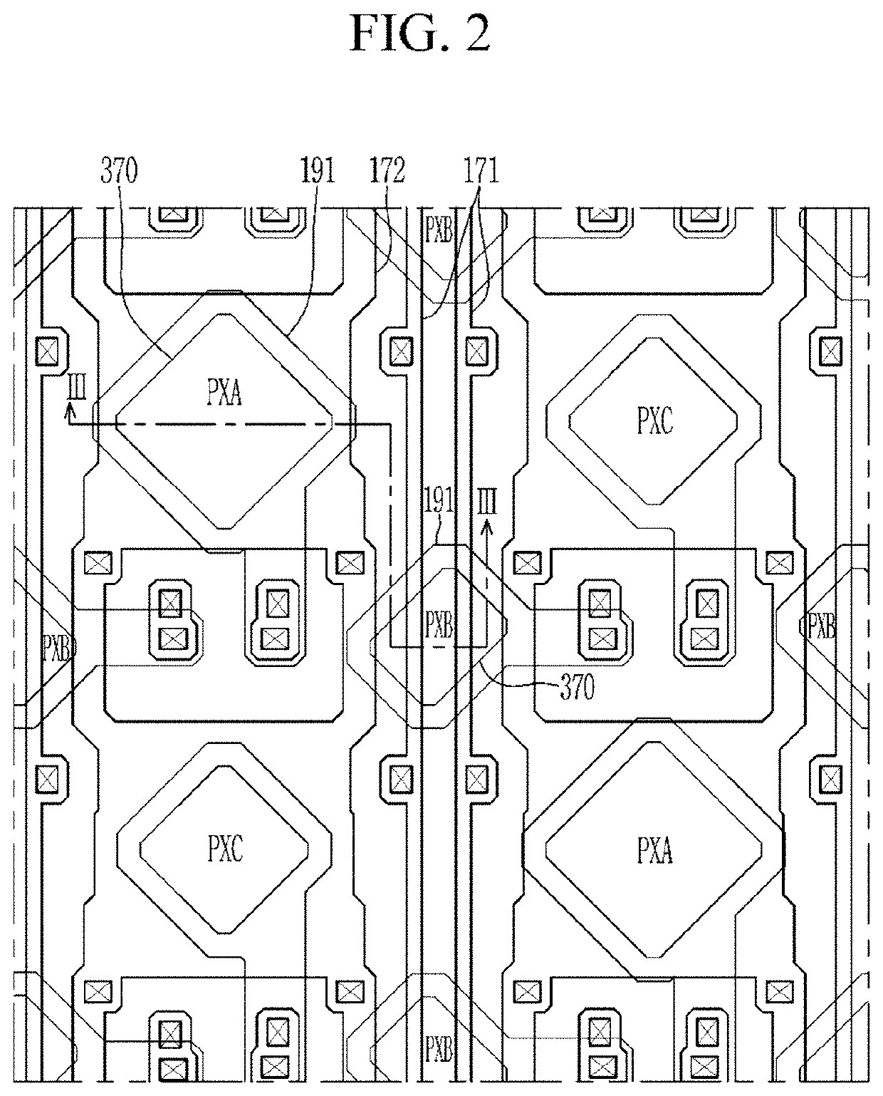
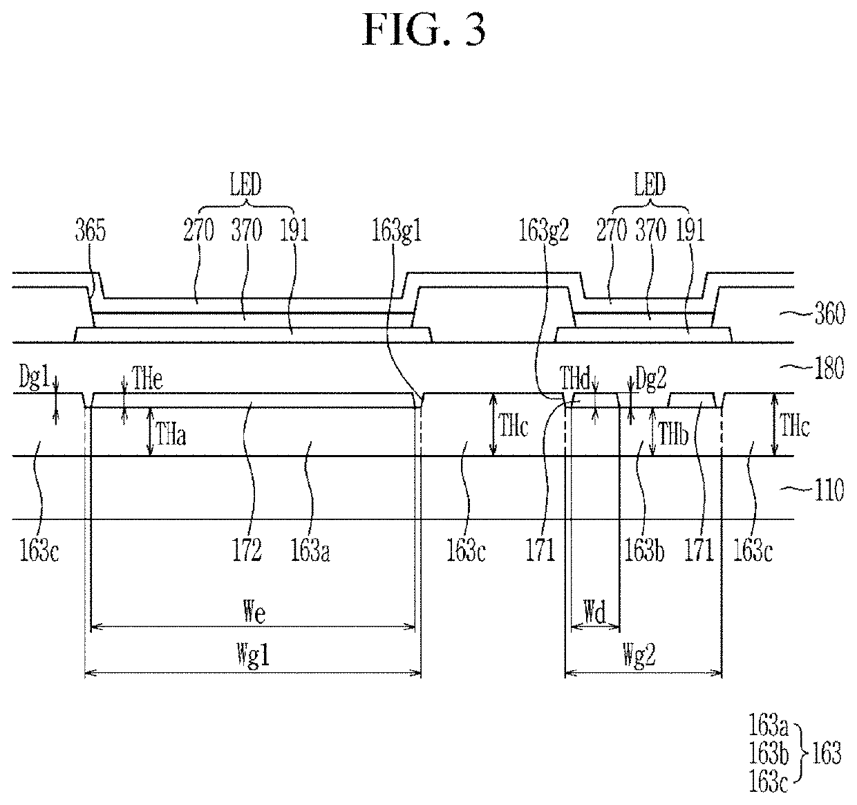
[0065]Example embodiments are described with reference to the accompanying drawings. The described embodiments may be modified in various ways.

[0066]In the application, identical or similar elements may be denoted by the same reference numerals or identifiers.

[0067]In the drawings, dimensions may be exaggerated for clarity.

[0068]Although the terms “first,”“second,” etc. may be used to describe various elements, these elements should not be limited by these terms. These terms may be used to distinguish one element from another element. A first element may be termed a second element without departing from teachings of one or more embodiments. The description of an element as a “first” element may not require or imply the presence of a second element or other elements. The terms “first,”“second,” etc. may be used to differentiate different categories or sets of elements. For conciseness, the terms “first,”“second,” etc. may represent “first-category (or first-set),”“second-category (or...


PUM


Abstract

A display device includes a substrate, a transistor, an interlayer insulating layer, a first conductive line, a pixel electrode, a passivation layer, a common electrode, and a light emitting element layer. The transistor overlaps the substrate. The interlayer insulating layer overlaps the transistor and includes a first groove. The first conductive line is electrically connected to the transistor and is at least partially disposed inside the first groove. The pixel electrode is electrically connected to the transistor and overlaps the first conductive line. The passivation layer is disposed between the pixel electrode and the first conductive line and directly contacts at least one of the pixel electrode and the first conductive line. The common electrode overlaps the pixel electrode. The light emitting element layer is disposed between the common electrode and the pixel electrode.

Description

CROSS-REFERENCE TO RELATED APPLICATION[0001]This application claims priority to and the benefit of Korean Patent Application No. 10-2020-0115379 filed in the Korean Intellectual Property Office on Sep. 9, 2020; the Korean Patent Application is incorporated by reference.BACKGROUND1. Field[0002]The technical field relates to a display device.2. Description of the Related Art[0003]A display device may display images according to input signals. Modern display devices include liquid crystal display (LCD) devices and organic light emitting diode (OLED) display devices. Display devices may be included in various electronic devices, such as mobile phones, navigation devices, digital cameras, electronic books, and portable game machines.[0004]Typically, external light incident on an OLED display device may be reflected on one or more internal surfaces of the OLED display device, undesirably reducing contrast of displayed images. As a result, the image display quality of the OLED display devi...

Claims


Application Information

Patent Timeline
IPC IPC(8): H01L27/32H01L51/52
CPCH01L27/3276H01L27/322H01L27/3246H01L27/3272H01L51/5253H10K59/122H10K59/131H10K59/8792H10K59/8731H01L27/1225H10K59/124H10K2102/351G09G3/3225H10K59/38H10K59/40H10K50/844H10K59/126
Inventor LEE, JUN HEECHOI, NAK CHORYU, MIN YEULLEEIM, CHOONG YOULCHOI, BEOHM ROCK
Owner SAMSUNG DISPLAY CO LTD
Why Eureka
Try Eureka