Organic light-emitting display device

Active Publication Date: 2018-07-05
LG DISPLAY CO LTD
View PDF6 Cites 13 Cited by
  • Summary
  • Abstract
  • Description
  • Claims
  • Application Information

AI Technical Summary

Benefits of technology

This patent aims to create an organic light-emitting display that can prevent outside light from reflecting and improve the clarity of transparent displays.

Problems solved by technology

In organic light-emitting display devices that realize such a transparent display, a polarizing plate for reducing the reflection of external light cannot be used.
As a result, transparent top-emission type organic light-emitting display devices do not satisfactorily prevent the reflection of external light, which causes deterioration in the quality of images.

Method used


Image

  • Organic light-emitting display device
  • Organic light-emitting display device
  • Organic light-emitting display device

Examples


first embodiment

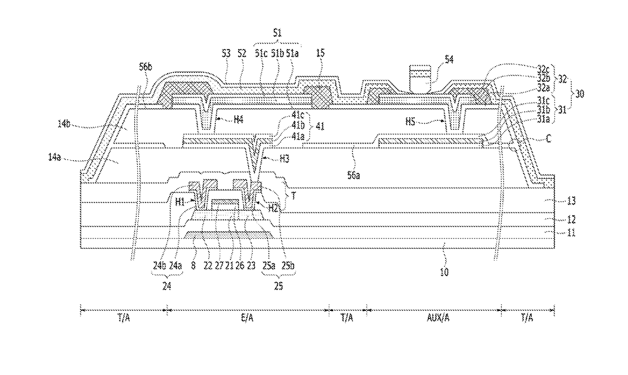
[0020]FIG. 1 is a schematic view illustrating an organic light-emitting display device according to the present disclosure.

[0021]The organic light-emitting display device according to the first embodiment of the present disclosure includes a thin film transistor T located on a first substrate 10, which is defined by a light emission area E / A and a transmission area T / A, a passivation layer 13 provided on the thin film transistor T, a planarization film 14 provided on the passivation layer 13, a first electrode 51 located on a region of the planarization film 14 corresponding to the light emission area E / A, the first electrode 51 being electrically connected to the thin film transistor T, an organic light emissive layer 52 provided on the first electrode 51, and a second electrode 53 provided on the organic light emissive layer 52. A shielding layer 56 is provided on a region of the planarization film 14 corresponding to the transmission area T / A. A black bank 15 is further provided ...

second embodiment

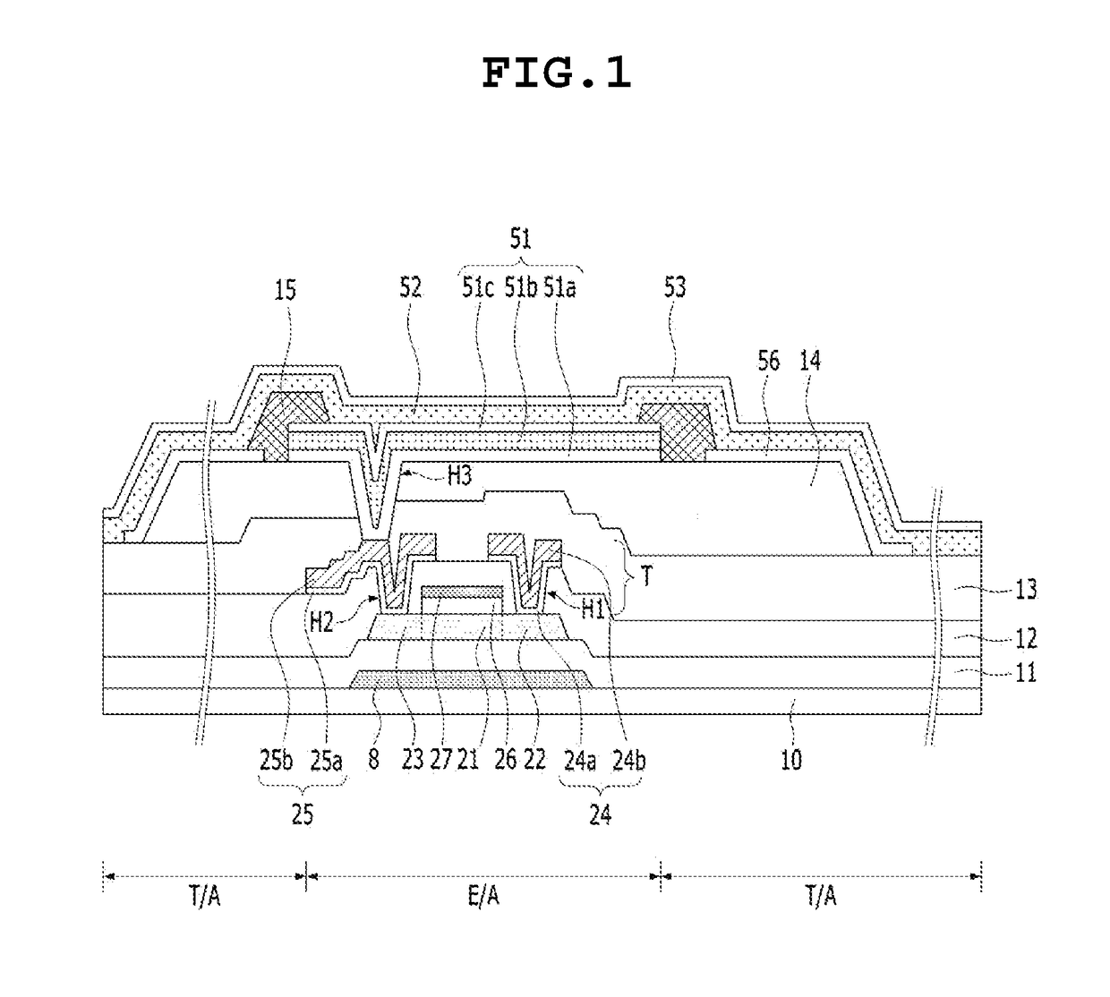
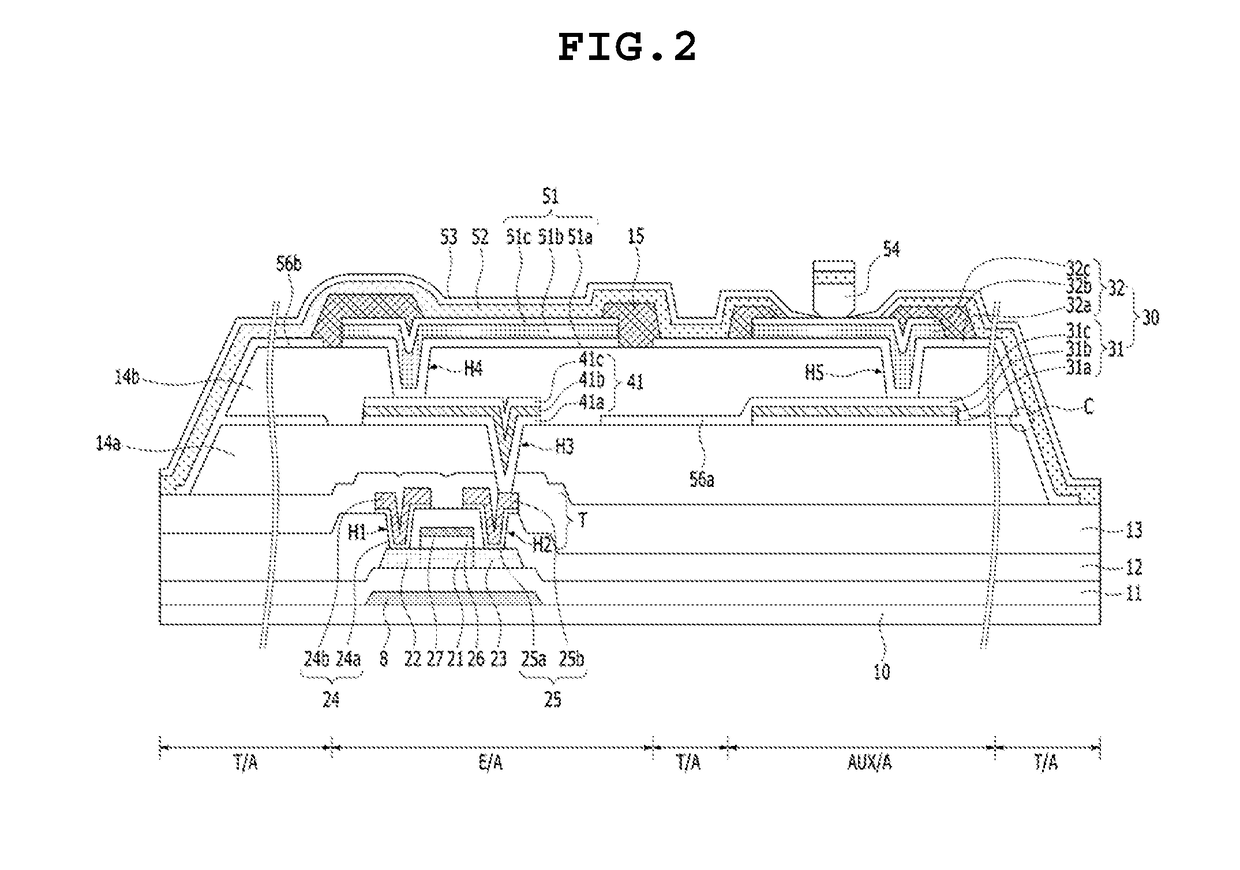
[0045]FIG. 2 is a schematic view illustrating an organic light-emitting display device including an auxiliary electrode and a connection electrode according to the present disclosure.

[0046]The organic light-emitting display device according to the second embodiment includes a thin film transistor T located on a first substrate 10, which is defined by an emission area E / A, a transmission area T / A, an auxiliary electrode area Aux / A, a passivation layer 13 provided on the thin film transistor T, a first planarization film 14a provided on the passivation layer 13, a connection electrode 41 located on the first planarization film 14a so as to contact the thin film transistor T, a second planarization film 14b for covering the connection electrode 41, a first electrode 51 located on a region of the second planarization film 14b corresponding to the emission area E / A, the first electrode 51 being electrically connected to the thin film transistor T, an organic light emissive layer 52 provi...


PUM


Abstract

Disclosed is an organic light-emitting display device that is capable of preventing the reflection of light incident from outside and improving transparency when a transparent display is realized. The organic light-emitting display device includes a first substrate defined by a transmission area and a light emission area, a first electrode located on a region of a planarization film, which covers a thin film transistor, corresponding to the light emission area, the first electrode being electrically connected to the thin film transistor, and a shielding layer located to cover a region of the planarization film corresponding to the transmission area and the side surface of the planarization film, the shielding layer being electrically isolated from the first electrode. A black bank is provided between the transmission area and the emission area so as to cover the edge of the first electrode, and an organic light emissive layer and a second electrode, which covers the organic light emissive layer, are sequentially formed on the first electrode.

Description

[0001]This application claims the benefit of Korean Patent Application No. 10-2016-0184484, filed on Dec. 30, 2016, which is hereby incorporated by reference as if fully set forth herein.BACKGROUNDTechnical Field[0002]The present disclosure relates to an organic light-emitting display device, and more particularly to an organic light-emitting display device that is capable of reducing the reflection of external light and improving transmittance when a transparent display is realized using the organic light-emitting display device.Description of the Related Art[0003]Image display devices, which are a core technology in the information and communication age and serve to display various kinds of information on a screen, have been developed such that the image display devices are thinner, lighter, and portable and exhibit high performance. In addition, organic light-emitting display devices, which control the amount of light that is emitted from an organic light-emitting layer to displa...

Claims


Application Information

Patent Timeline
IPC IPC(8): H01L51/52H01L27/32H01L51/56
CPCH01L51/56G02B5/003H01L27/3272H01L51/5284H01L27/3246H01L51/5228H01L27/3258H01L27/3262H01L2227/323H01L51/5215H01L27/3248H10K59/126H10K2102/3026H10K59/878H10K59/8792H10K59/1315H10K59/124H10K59/122H10K59/1201H10K59/123H10K59/1213H10K59/131H10K50/865H10K50/816H10K50/824H10K71/00
Inventor LEE, JAE-SUNGIM, JONG-HYEOKKIM, DO-HYUNG
Owner LG DISPLAY CO LTD
Why Eureka
Try Eureka