Eureka AIR delivers breakthrough ideas for toughest innovation challenges, trusted by R&D personnel around the world.

Bonded structures with integrated passive component

a passive component and bonding technology, applied in the direction of fixed capacitor details, fixed capacitors, fixed capacitor associations, etc., can solve the problem of challenging the efficiency of incorporating passive components

Active Publication Date: 2018-07-05
ADEIA SEMICON BONDING TECH INC
View PDF8 Cites 78 Cited by
  • Summary
  • Abstract
  • Description
  • Claims
  • Application Information

AI Technical Summary

Benefits of technology

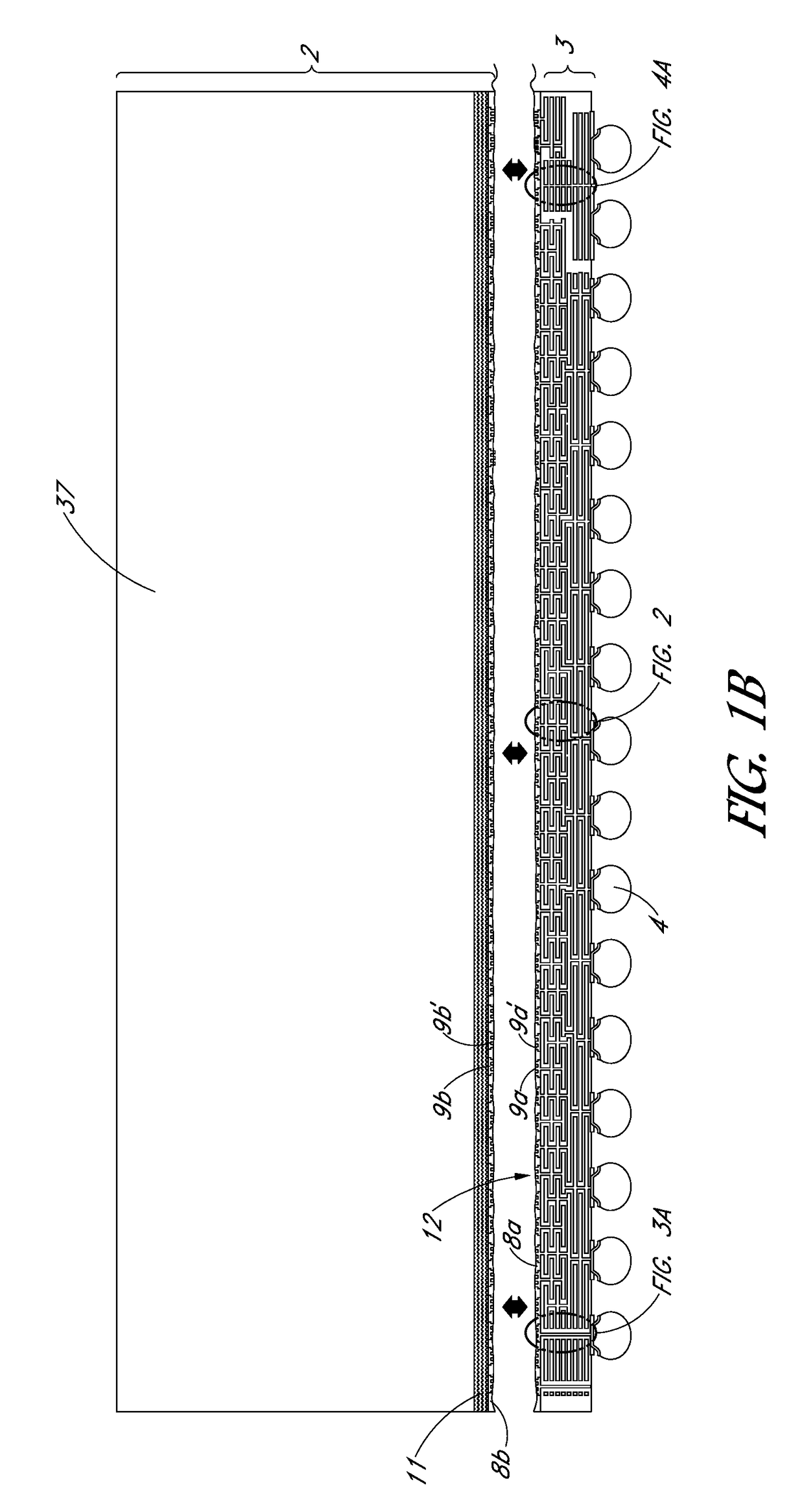
The patent text describes a method for incorporating passive electronic components into electronic systems in an efficient manner. The technical effects of the patent include improved incorporation of passive components into electronic systems, reduced space occupancy on the integrated device die, package, and system board, and increased performance of active devices of the system. The method involves forming a bonded structure with an integrated passive component, which includes a high K dielectric material to define a capacitive sheet. The bonded structure can be formed by directly bonding a semiconductor element to the passive component or by using a sacrificial base. The method also allows for the incorporation of power electrodes and ground electrodes in a passive electronic component. The patent text provides various schematic views and plots of transfer impedance as a function of frequency for different devices having different passive electronic components.

Problems solved by technology

Incorporating passive components in an efficient manner may be challenging, since the passive components occupy valuable space on the integrated device die, the package, and / or the system board.

Method used


Image

  • Bonded structures with integrated passive component
  • Bonded structures with integrated passive component
  • Bonded structures with integrated passive component

Examples


Embodiment Construction

[0067]Various embodiments disclosed herein related to a bonded structure comprising a semiconductor element and a passive electronic component directly bonded to the semiconductor element without an intervening adhesive. In various embodiments, the passive electronic component comprises a capacitor. In other embodiments, the passive electronic component can comprise other devices, such as an inductor, a resistor, a voltage regulator, a filter, and / or a resonator. Beneficially, the passive electronic component can be integrated into a layer of passive components that is directly bonded to the semiconductor element (such as an integrated device die). In the illustrated embodiments, for example, the layer of passive components can be disposed between the semiconductor element and another system component such as an interposer, system substrate, etc. The passive electronic component described herein can thereby reduce the space occupied by passive components at the integrated device, at...


PUM

PropertyMeasurementUnit
surface roughnessaaaaaaaaaa
degree of smoothnessaaaaaaaaaa
RMS roughnessaaaaaaaaaa

Abstract

In various embodiments, a bonded structure is disclosed. The bonded structure can include an element and a passive electronic component having a first surface bonded to the element and a second surface opposite the first surface. The passive electronic component can comprise a first anode terminal bonded to a corresponding second anode terminal of the element and a first cathode terminal bonded to a corresponding second cathode terminal of the element. The first anode terminal and the first cathode terminal can be disposed on the first surface of the passive electronic component.

Description

CROSS-REFERENCE TO RELATED APPLICATIONS[0001]This application claims priority to U.S. Provisional Patent Application No. 62 / 440,161, filed Dec. 29, 2016, and to U.S. Provisional Patent Application No. 62 / 518,472, filed Jun. 12, 2017, the entire contents of each of which are incorporated by reference herein in their entirety and for all purposes.[0002]This application is also related to U.S. patent application Ser. No. 15 / 426,942, filed Feb. 7, 2017, which is incorporated by reference herein in its entirety and for all purposes.BACKGROUNDField[0003]The field relates to bonded structures with integrated passive components.Description of the Related Art[0004]Passive electronic components, such as capacitors, resistors, and inductors, play important roles in electronic systems. For example, passive components help smooth signals and increase the performance of active devices of the system. Incorporating passive components in an efficient manner may be challenging, since the passive comp...

Claims


Application Information

Patent Timeline
Patent Type & Authority Applications(United States)
IPC IPC(8): H01L23/498H01L23/00H01L23/66H01G4/30H01G4/228H01G4/12H01G4/38H01G4/40H05K1/18H10N97/00
CPCH01L23/49838H01L23/49816H01L24/05H01L24/08H01L24/32H01L23/66H01L23/49827H01G4/30H01G4/228H01G4/1245H01G4/38H01G4/40H05K1/18H01L2924/19103H01L2223/6666H01L2223/6672H01L2924/19041H01L2924/19011H01L2224/05005H01L2224/05017H01L2224/0807H01L2224/08265H01L2224/32265H05K2201/10015H05K1/0231H05K1/185H01L2224/16265H01L24/80H01L2224/03845H01L2224/05556H01L2224/05567H01L2224/05647H01L2224/05686H01L2224/80895H01L2224/80896H01L2224/80203H01L2224/05576H01L2224/80948H01G2/02H01L23/48H01L23/49822H01L23/5223H01L2924/00014H01L2924/05442H01L2924/00012
Inventor HABA, BELGACEMMOHAMMED, ILYASKATKAR, RAJESHGUEVARA, GABRIEL Z.DELACRUZ, JAVIER A.HUANG, SHAOWUMIRKARIMI, LAURA WILLS
Owner ADEIA SEMICON BONDING TECH INC
Why Eureka
Eureka Blog
Learn More