Optical transmission device and control method therefor
a transmission device and optical technology, applied in optics, instruments, electrical equipment, etc., can solve the problems of iq modulator dc bias drift, iq modulator operation inaccurately, transmission signal degradation of iq modulator, etc., to achieve stable and highly reliable modulated optical signals
- Summary
- Abstract
- Description
- Claims
- Application Information
AI Technical Summary
Benefits of technology
Problems solved by technology
Method used
Image
Examples
first example embodiment
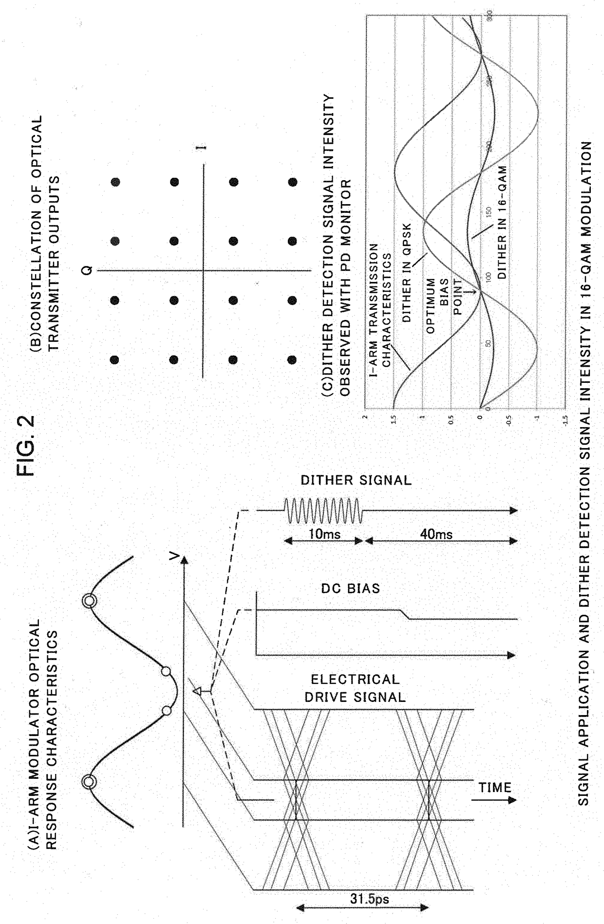
[0106]A first example embodiment is based on a finding (results of experiments by the present inventors) that since a noise component produced by I / Q quadrature skew is mixed in bias control for an I-arm or Q-arm in an optical transmitter that includes a multilevel modulation unit such as a 16-QAM modulation unit, the stability of the I-arm or the Q-arm control can be increased by observing I / Q quadrature skew concurrently and removing the noise component from a bias control signal for the I-arm or the Q-arm.
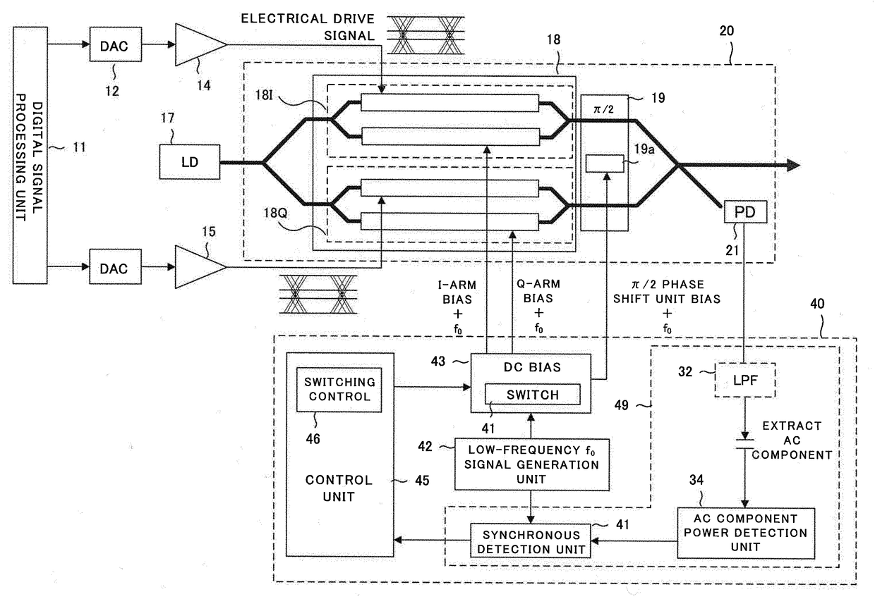
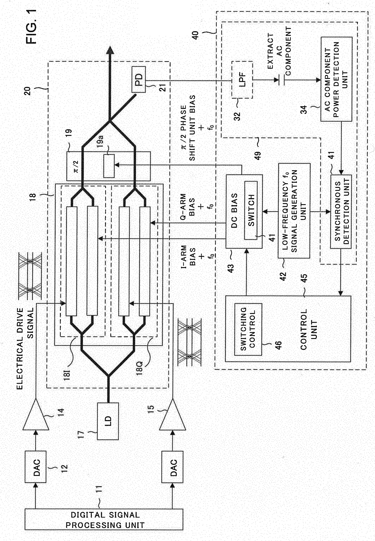
[0107]FIG. 6 is a diagram illustrating a configuration of an optical transmitter 129 of a first example embodiment. In the first example embodiment, 16-QAM modulation is applied to an optical modulator (IQ modulator) 105 and a portion of its output light is extracted as a monitor signal. A control signal is generated from the monitor signal to control biases of an I-arm and a Q-arm and a bias of an optical π / 2 phase shift unit 108.
[0108]The optical transmitter 129 includes a las...
second example embodiment
[0207]FIG. 14 is a diagram illustrating a configuration of an optical transmitter according to a second example embodiment. Differences form the first example embodiment in FIG. 6 are:[0208]a method of superimposing a dither signal on an optical π / 2 phase shift unit 108,[0209]a method of acquiring a control signal for I / Q quadrature control, and[0210]an ABC control circuit schedule.
[0211]I / Q quadrature control operation is performed along with bias control for an I-arm modulator and a Q-arm modulator, thereby reducing control sequence time and start-up time of an optical transmitter 144, and stabilizing an ABC circuit.
[0212]In FIG. 14, a dither signal cut from a signal from a low-frequency oscillator 117 is not superimposed on a bias signal 126 (bias signal 126 to an optical π / 2 phase shift unit 108) output from a DC bias generation unit 122 in a control unit 142.
[0213]The dither signal is superimposed on a bias signal 124 for an I-arm modulator 106 and a bias signal 125 for a Q-arm...
third example embodiment
[0224]FIG. 16 is a diagram illustrating a configuration of an optical transmitter of a third example embodiment. The third example embodiment differs from the first example embodiment in FIG. 6 in that in place of the noise remover 120, a control value selector 151 is provided in a control unit 153 to simplify the control process of the control unit 153, thereby providing an ABC circuit 154 aimed to achieve stable operation.
[0225]In the third example embodiment in FIG. 16, an RMS detection value 115 from a signal amplitude detector 114 is selected and output as a noise component 131, which is one of outputs of a noise component detector 119 in the control unit 153. For the control value selector 151 into which the noise component 131 is input, a threshold input unit 152 is provided as another input signal source.
[0226]On the other hand, as a control signal 132, which is another output of the noise component detector 119, an envelope detection signal 116 from the signal amplitude det...
PUM
| Property | Measurement | Unit |
|---|---|---|
| quadrature angle | aaaaa | aaaaa |
| I/Q quadrature angle | aaaaa | aaaaa |
| I/Q quadrature angle | aaaaa | aaaaa |
Abstract
Description
Claims
Application Information
 - R&D
- Intellectual Property
- Life Sciences
- Materials
- Tech Scout
- Unparalleled Data Quality
- Higher Quality Content
- 60% Fewer Hallucinations
Browse by: Latest US Patents, China's latest patents, Technical Efficacy Thesaurus, Application Domain, Technology Topic, Popular Technical Reports.
© 2025 PatSnap. All rights reserved.Legal|Privacy policy|Modern Slavery Act Transparency Statement|Sitemap|About US| Contact US: help@patsnap.com


