Piezoresistive Device
a technology of piezoresistive devices and conductive materials, which is applied in the direction of measuring devices, instruments, non-conductive materials with dispersed conductive materials, etc., can solve the problems of inability to measure small forces, instant drop in resistance from infinite resistance, and device suffer from a number of drawbacks, so as to speed up the drying of ink
- Summary
- Abstract
- Description
- Claims
- Application Information
AI Technical Summary
Benefits of technology
Problems solved by technology
Method used
Image
Examples
example 1
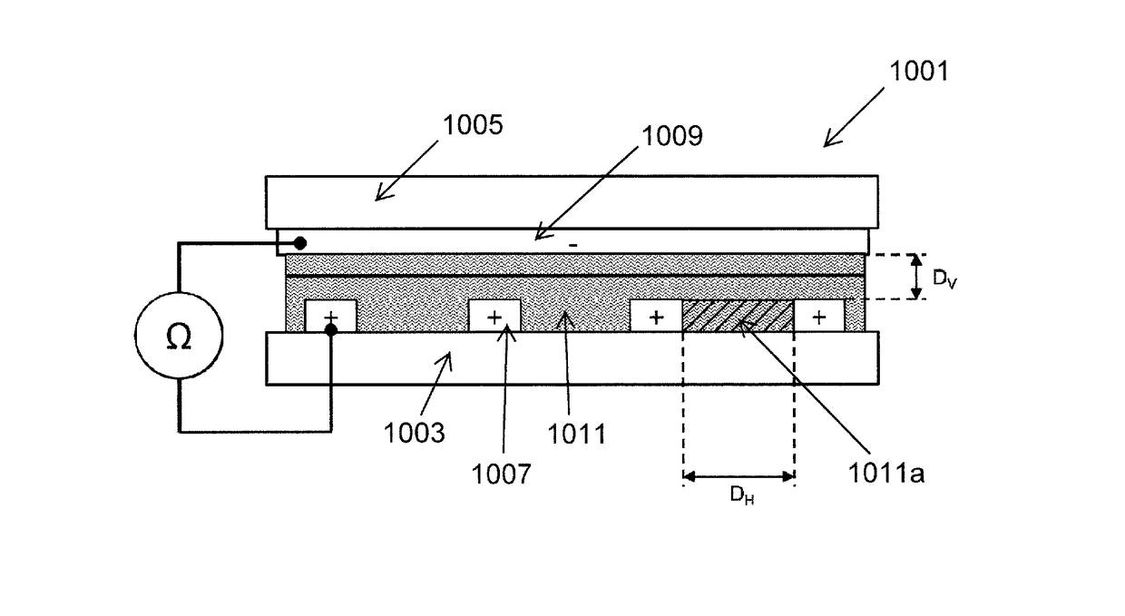
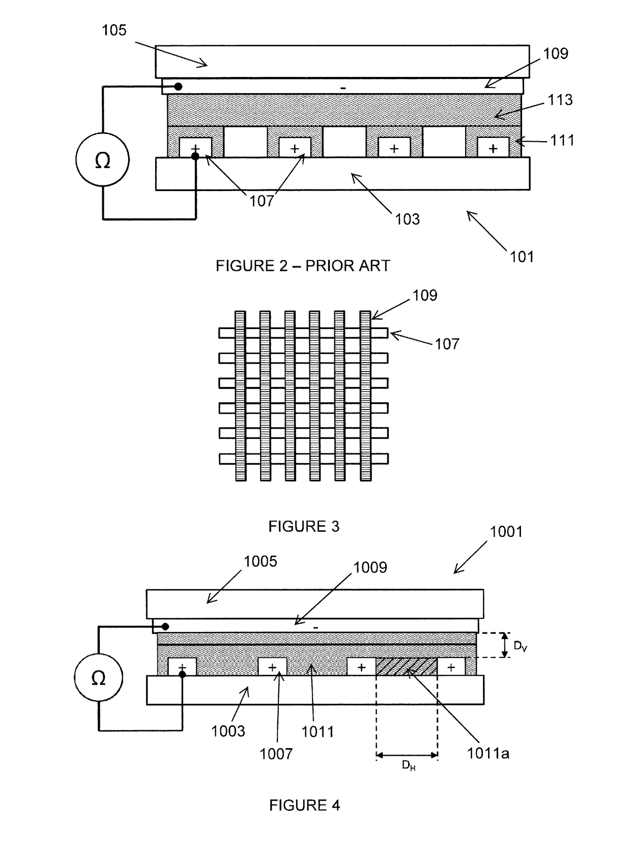
[0105]A piezoresitive device was produced and measured according to the different layer measurement mode described above, in order to assess the piezoresistive properties of a high aspect ratio carbon nanoparticle ink.
[0106]Two 10 mm by 9 cm strips of a conductive silver ink (AG 500, Conductive Compounds PE) were screen printed onto a PET substrate (175 μm thickness) using a DEK 248 screen printer. Each strip was then overprinted with three layers of piezoresistive ink containing carbon nanoparticles including functionalised GNPs (Haydale Graphene Industries plc) in a polymer matrix and solvent, whilst leaving a small area of the conductive silver exposed at one end. Each piezoresistive ink layer was dried before the application of subsequent ink layers. The assembly was then cut in half (each bearing a silver strip), and the two halves overlaid with the piezoresistive ink layers facing one another, so as to form a piezoresistive sensor.
[0107]To measure the resistance behaviour of t...
example 2
[0111]Experiments broadly following a similar protocol to that described for Example 1 were carried out using piezoresistive ink containing carbon nanoparticles including functionalised GNPs in a vinyl chloride copolymer based binder.
[0112]In this case silver traces of 20 mm width, 150 mm length and ˜8 μm height were screen printed with a 54 / 64 mesh onto a 330 μm thick PET substrate using a DEK 248 screen printer. Three layers of piezoresistive ink were printed as continuous blocks over the silver traces using a 54 / 64 mesh to give a total height of ˜9 μm. A piezoresistive device was then formed following the same approach as in Example 1, and the resistance measured over a circular area with a diameter 15 mm (1.77 cm2 area of compression). Three different devices were produced having “high”, “medium” and “low” loadings of carbon nanoparticles in the piezoresistive material. The devices having medium and low loadings had four and eight times less carbon than the high loading respecti...
example 3
[0114]Experiments were carried out to determine the effect of increasing the number of layers of piezoresistive ink on resistance, with results shown in FIG. 10.
[0115]A series of lower substrates were produced by screen printing an indium tin oxide sheet with one, two or three layers of a piezoresistive ink containing 3.5 wt. % functionalised graphene nanoplatelets (with negligible content of other types of carbon particle) dispersed in vinyl chloride copolymer based binder and solvent (15 parts binder to 85 parts solvent). The dried ink had a GNP content of ˜20 wt. %. Piezoresistive devices were formed by combining the lower substrates with an upper substrate, consisting of a further indium tin oxide sheet optionally bearing a single layer of the same piezoresistive ink as the lower substrate. The resistance of these devices under an applied pressure of 2000 N was measured using a Housfield extensometer with a circular area of compression of 1.77 cm2 (diameter 15 mm)
[0116]As can be...
PUM
 Abstract
Description
Claims
Application Information
 - R&D
- Intellectual Property
- Life Sciences
- Materials
- Tech Scout
- Unparalleled Data Quality
- Higher Quality Content
- 60% Fewer Hallucinations
Browse by: Latest US Patents, China's latest patents, Technical Efficacy Thesaurus, Application Domain, Technology Topic, Popular Technical Reports.
© 2025 PatSnap. All rights reserved.Legal|Privacy policy|Modern Slavery Act Transparency Statement|Sitemap|About US| Contact US: help@patsnap.com


