APPLICATION OF eBIP TO INSPECTION, TEST, DEBUG AND SURFACE MODIFICATIONS

Inactive Publication Date: 2017-10-12
ORBOTECH LTD +1
View PDF4 Cites 6 Cited by
  • Summary
  • Abstract
  • Description
  • Claims
  • Application Information

AI Technical Summary

Benefits of technology

The patent describes an invention that uses electron-beam induced plasmas (eBIP) to create a non-mechanical, electrical contact with a device of interest and to stimulate a sample for analysis. The eBIP plasma source is created by extracting an electron beam from an electron source and transmitting it into an adjacent gas ambient to ionize the gas molecules around it. The plasma is then used to pass an electrical signal to an external measurement apparatus, providing a sensor for the amount of current generated by the stimulus of the electron beam. The invention has various applications, such as voltage contrast imaging and inspecting material composition profile of a sample.

Problems solved by technology

They may roughly be divided into two categories, one category being based on high intensity laser-induced ionization, which presents possible risks of laser-induced damage to the device under tests given the high ionization thresholds, and another category being based on high voltage corona discharges, in which ionized species have a wide range of scattering angles (little directional control) and also presents damage risks, especially related to arcing.
This technology involves large vacuum enclosures and complex electron optics, leading to high system costs, large factory foot prints and potentially impacting throughput.

Method used


Image

  • APPLICATION OF eBIP TO INSPECTION, TEST, DEBUG AND SURFACE MODIFICATIONS
  • APPLICATION OF eBIP TO INSPECTION, TEST, DEBUG AND SURFACE MODIFICATIONS
  • APPLICATION OF eBIP TO INSPECTION, TEST, DEBUG AND SURFACE MODIFICATIONS

Examples


Embodiment Construction

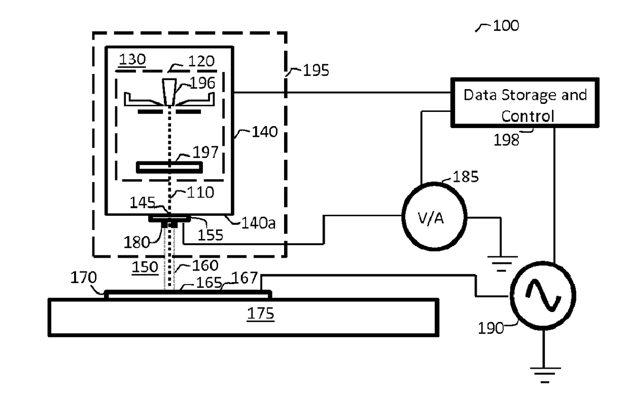
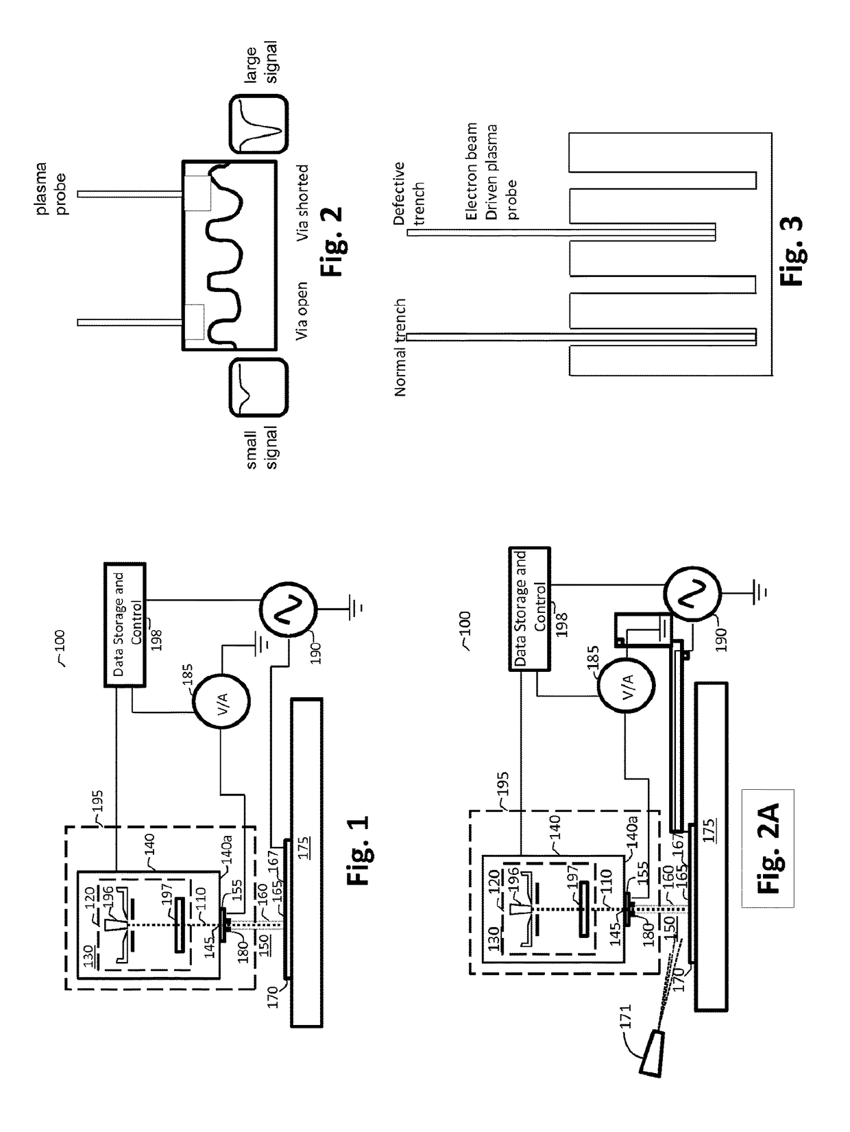
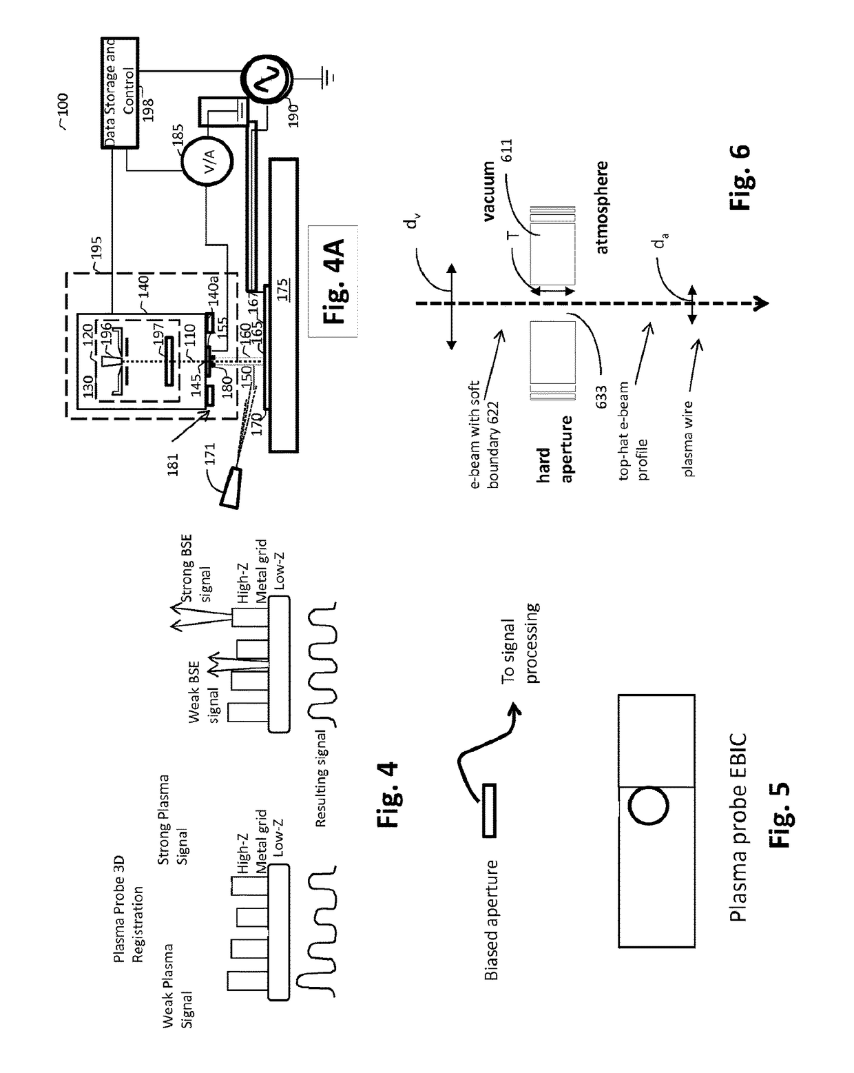
[0047]Various embodiments described below provide solutions based on a high resolution, high sensitivity, and compact atmospheric electron beam induced plasma probe technology. This technology essentially relies on the fact that the plasma generated by collisional ionization events driven by the electron beam in air acts as a non-mechanical conductive contact, allowing voltages on the devices under test (DUT) to be measured via the resulting secondary plasma electron current. As implied by the name, this technology does not require the DUT to be held in vacuum. Rather, only the electron emitter (cathode) and electron optics need to be kept in a vacuum enclosure. Furthermore, the implementation of this technology only requires simple electron optics configurations, e.g. an extraction grid and an electrostatic lens, keeping the gun cost low and its size, and hence the size of the enclosure, compact. The electron beam exits the vacuum enclosure containing the electron gun into the surr...


PUM


Abstract

An electron-beam induced plasma is utilized to establish a non-mechanical, electrical contact to a device of interest. This plasma source may be referred to as atmospheric plasma source and may be configured to provide a plasma column of very fine diameter and controllable characteristics. The plasma column traverses the atmospheric space between the plasma source into the atmosphere and the device of interest and acts as an electrical path to the device of interest in such a way that a characteristic electrical signal can be collected from the device. Additionally, by controlling the gases flowing into the plasma column the probe may be used for surface modification, etching and deposition.

Description

CROSS-REFERENCES TO RELATED APPLICATIONS[0001]The present application claims priority benefit from U.S. Provisional Application, Ser. No. 62 / 051,871, filed on Sep. 17, 2014, which claims priority benefit from U.S. Provisional Application, Ser. No. 61 / 886,625, filed on Oct. 3, 2013, and is also relates to PCT application number WO2013 / 012616, filed Jul. 10, 2012, entitled “ELECTRICAL INSPECTION OF ELECTRONIC DEVICES USING ELECTRON-BEAM INDUCED PLASMA PROBES”, the content of both of which is incorporated herein by reference in its entirety.BACKGROUND1. Field[0002]Various embodiments of the present invention generally relate to the non-mechanical contact probing of electronic devices and surface modification of devices and tissue. In particular, the various embodiments relate to application of electron-beam induced plasma probes for metrology and surface modification.2. Related Arts[0003]The ability to measure and apply voltages and currents on patterned structures without having to es...

Claims


Application Information

Patent Timeline
IPC IPC(8): H01J37/32
CPCH01J37/32825H05H2240/10
Inventor SALEH, NEDALSTERLING, UNIT BTOET, DANIELGLAZER, ARIELOEWINGER, RONENKRISHNASWAMI, SRIRAM
Owner ORBOTECH LTD
Why Eureka
Try Eureka