Semiconductor device, display device including the semiconductor device, display module including the display device, and electronic appliance including the semiconductor device, the display device, and the display module
a technology of semiconductor devices and semiconductor devices, applied in the direction of semiconductor devices, transistors, electrical devices, etc., can solve the problems of affecting the characteristics of transistors, image quality of display devices, and large occupation area of inverted staggered transistors, so as to achieve low manufacturing cost, signal delay, and relatively simple manufacturing process
- Summary
- Abstract
- Description
- Claims
- Application Information
AI Technical Summary
Benefits of technology
Problems solved by technology
Method used
Image
Examples
embodiment 1
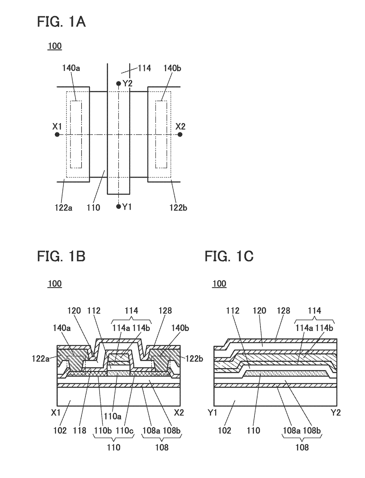
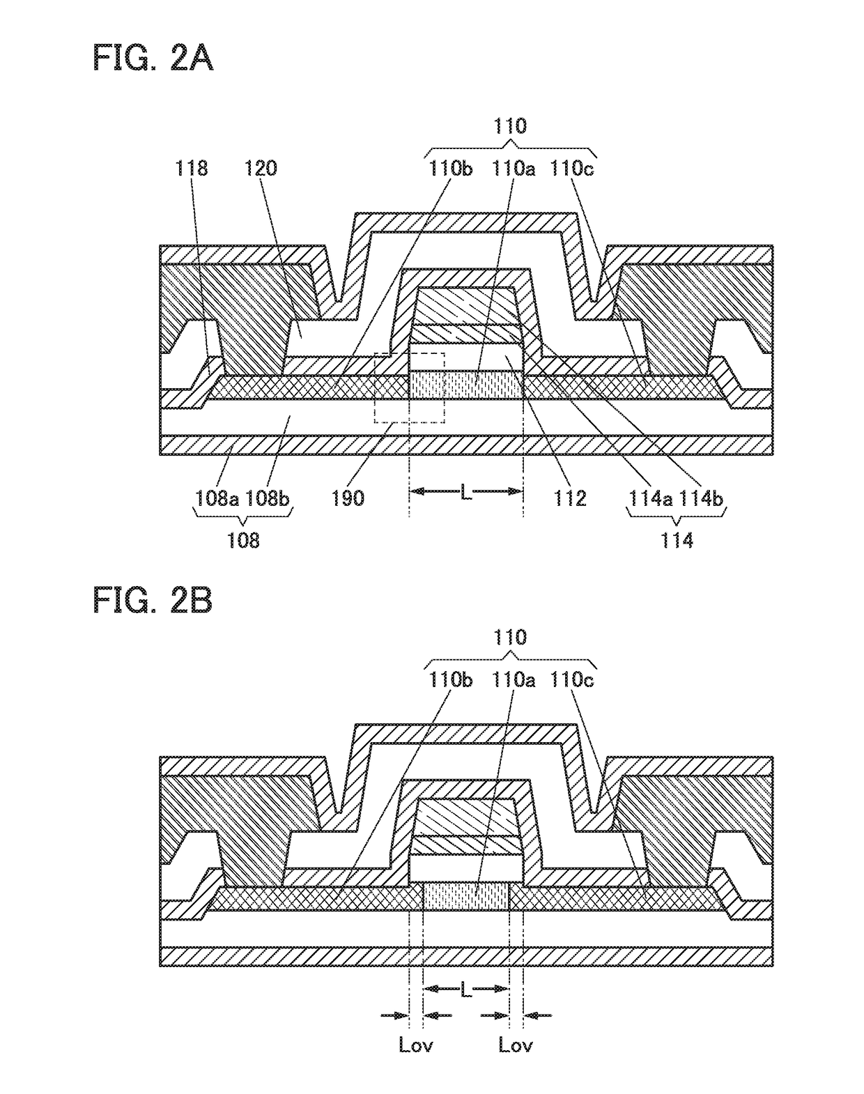
[0070]In this embodiment, examples of a semiconductor device including a transistor and a method for manufacturing the semiconductor device are described with reference to FIGS. 1A to 1C, FIGS. 2A and 2B, FIG. 3, FIGS. 4A and 4B, FIGS. 5A to 5C. FIGS. 6A to 6C, FIGS. 7A to 7D, FIGS. 8A to 8D, FIGS. 9A to 9D, and FIGS. 10A and 10B.
[0071]FIGS. 1A to 1C illustrate an example of a semiconductor device including a transistor. Note that the transistor illustrated in FIGS. 1A to 1C has a top-gate structure.
[0072]FIG. 1A is a top view of a transistor 100 included in the semiconductor device. FIG. 1B is a cross-sectional view along the dashed-dotted line X1-X2 in FIG. 1A. FIG. 1C is a cross-sectional view along the dashed-dotted line Y1-Y2 in FIG. 1A. Note that in FIG. 1A, a substrate 102, an insulating film 108, an insulating film 112, and the like are omitted for simplicity. In a manner similar to that of FIG. 1A, some components are not illustrated in some cases in top views of transistor...
embodiment 2
[0258]In this embodiment, the structure of an oxide semiconductor included in a semiconductor device of one embodiment of the present invention is described below in detail.
[0259]First a structure of an oxide semiconductor film is described below.
[0260]An oxide semiconductor is classified into a single crystal oxide semiconductor and a non-single-crystal oxide semiconductor. Examples of a non-single-crystal oxide semiconductor include a c-axis aligned crystalline oxide semiconductor (CAAC-OS), a polycrystalline oxide semiconductor, a nanocrystalline oxide semiconductor (nc-OS), an amorphous-like oxide semiconductor (a-like OS), and an amorphous oxide semiconductor.
[0261]From another perspective, an oxide semiconductor is classified into an amorphous oxide semiconductor and a crystalline oxide semiconductor. Examples of a crystalline oxide semiconductor include a single crystal oxide semiconductor, a CAAC-OS, a polycrystalline oxide semiconductor, and an nc-OS.
[0262]It is known that ...
embodiment 3
[0355]In this embodiment, an oxygen vacancy of an oxide semiconductor film is described in detail below.
oH>
[0356]In the case where an oxide semiconductor film (hereinafter referred to as IGZO) is a complete crystal, H preferentially diffuses along the a-b plane at a room temperature. In heat treatment at 450° C., H diffuses along the a-b plane and in the c-axis direction. Here, description is made on whether H easily enters an oxygen vacancy Vo if the oxygen vacancy Vo exists in IGZO. A state in which H is in an oxygen vacancy Vo is referred to as VoH.
[0357]An InGaZnO4 crystal model shown in FIG. 26 was used for calculation. The activation barrier (Ea) along the reaction path where H in VoH is released from Vo and bonded to oxygen was calculated by a nudged elastic band (NEB) method. The calculation conditions are shown in Table 2.
TABLE 2SoftwareVASPCalculation methodNEB methodFunctionalGGA-PBEPseudopotentialPAWCut-off energy500 eVK points2 × 2 × 3
[0358]In the InGaZnO4 crystal model...
PUM
 Abstract
Description
Claims
Application Information
 - R&D
- Intellectual Property
- Life Sciences
- Materials
- Tech Scout
- Unparalleled Data Quality
- Higher Quality Content
- 60% Fewer Hallucinations
Browse by: Latest US Patents, China's latest patents, Technical Efficacy Thesaurus, Application Domain, Technology Topic, Popular Technical Reports.
© 2025 PatSnap. All rights reserved.Legal|Privacy policy|Modern Slavery Act Transparency Statement|Sitemap|About US| Contact US: help@patsnap.com


