
Optically transparent conductive material

a technology of conductive materials and transparent materials, applied in the direction of dielectric characteristics, circuit optical details, instruments, etc., can solve the problems of line breakage sensor parts tend to be charged, etc., and achieve the effect of improving the yield in the production of touchscreens and preventing the electrostatic destruction of peripheral wire parts

Inactive Publication Date: 2017-05-18
MITSUBISHI PAPER MILLS LTD
View PDF3 Cites 3 Cited by
  • Summary
  • Abstract
  • Description
  • Claims
  • Application Information

AI Technical Summary

Benefits of technology

The patent text describes a way to prevent damage to a touchscreen caused by static electricity. This is done by eliminating the electrical potential difference between different parts of the screen. This results in a better yield of optically transparent conductive material used in touchscreen production.

Problems solved by technology

If the line widths are thin and the intervals between the lines are narrow, a flaw occurring in the production process may cause a line break.
The protective film for such a use is prone to be charged, and therefore, when the surface of the optically transparent conductive material is covered with a protective film, the charge can move from the protective film to the sensor parts, and as a result the sensor parts tend to be charged.
In addition, when the protective film is removed from the optically transparent conductive material, the sensor parts tend to be charged.
Such discharge causes damage to the peripheral wire part (electrostatic destruction), resulting in a significantly reduced yield in the production of touchscreens.
However, before the stage of connection to the controller IC, for example, in a step of assembly or storage of optically transparent conductive materials not connected to the controller IC, it is extremely difficult to prevent the occurrence of electrical potential difference between charged sensor parts, which difference can cause electrostatic destruction of the peripheral wire part.

Method used

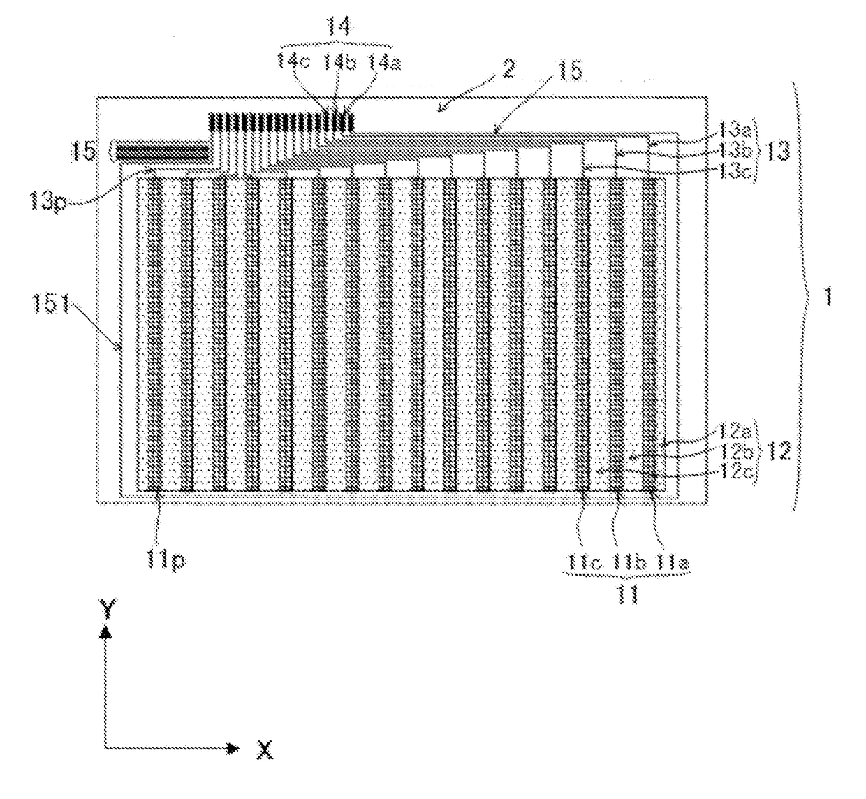
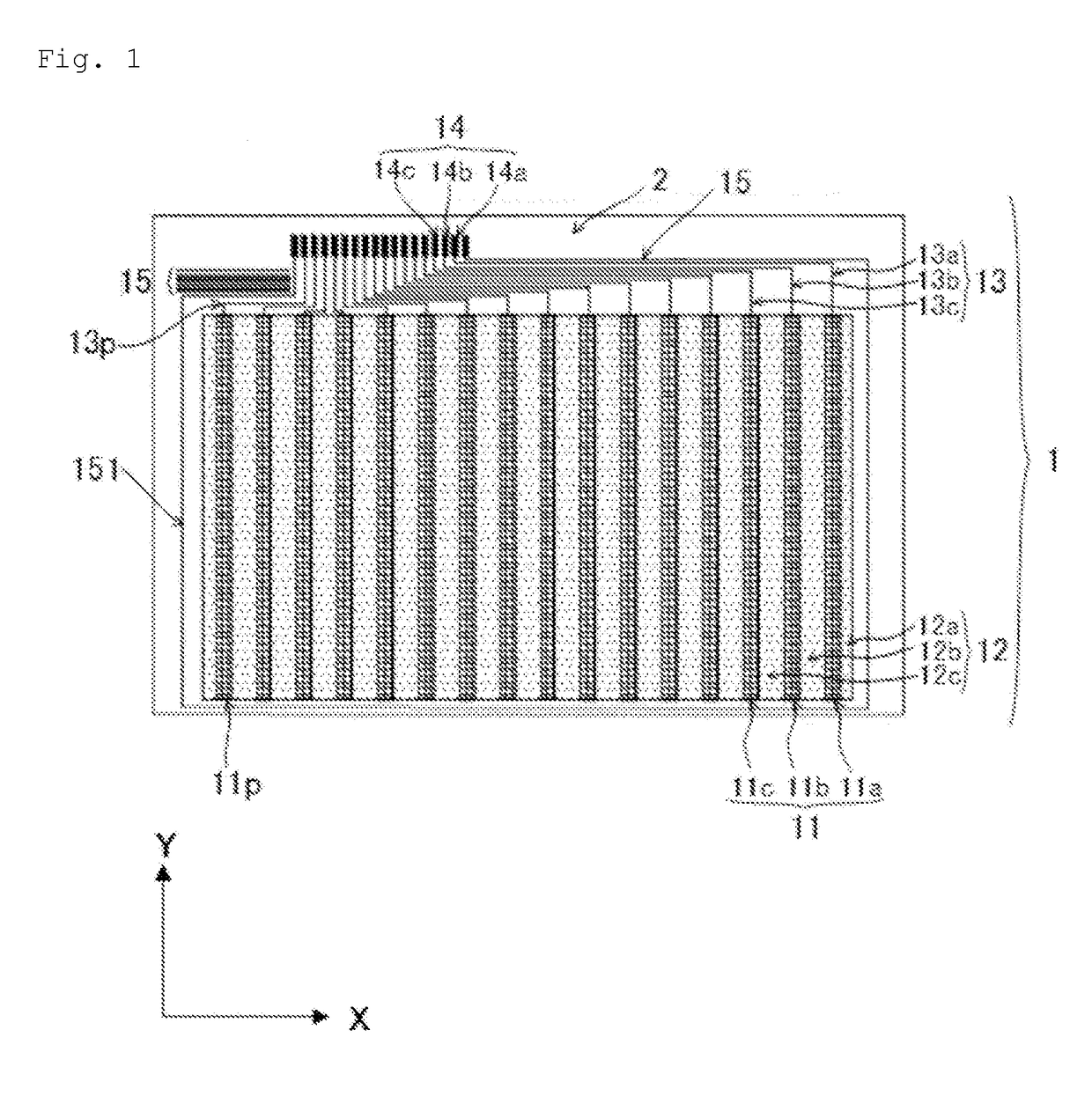
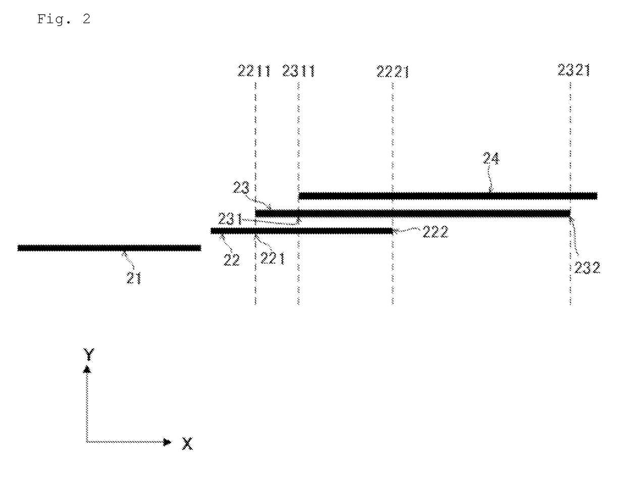

Image

  • Optically transparent conductive material
  • Optically transparent conductive material
  • Optically transparent conductive material

Examples


examples

[0040]Hereinafter, the present invention will be illustrated in more detail by Examples, but the present invention is not limited thereto and can be embodied in various ways within the scope of the invention.

1>

[0041]As a support, a 100-μm-thick polyethylene terephthalate film was used. The total light transmittance of this support was 91%.

[0042]Next, in accordance with the following formulation, a physical development nuclei coating liquid was prepared, applied onto the support, and dried to provide a physical development nuclei layer.

[0043]

Liquid APalladium chloride5gHydrochloric acid40mLDistilled water1000mLLiquid BSodium sulfide8.6gDistilled water1000mL

[0044]Liquid A and Liquid B were mixed with stirring, and after 30 minutes, passed through a column filled up with an ion exchange resin to give a palladium sulfide sol.

per m2 of Silver Halide Photosensitive Material

[0045]

The above-prepared palladium sulfide sol0.4mg2 mass % glyoxal aqueous solution0.2mLSurfactant (S-1)4mgPolyethyl...


PUM


Abstract

Provided is an optically transparent conductive material with which the yield in the production of touchscreens is improved can be provided. The optically transparent conductive material has, on a support, optically transparent sensor parts, optically transparent dummy parts, a terminal part, a peripheral wire part electrically connecting the sensor parts and the terminal part, and an earth part, the peripheral wire part having a parallel portion in which adjacent peripheral wires are parallel with each other, the earth part having a parallel portion in which adjacent earth wires are parallel with each other, an inequality A>B being satisfied when A is the smallest interval distance between peripheral wires in the parallel portion of the peripheral wire part and B is the smallest interval distance between earth wires in the parallel portion of the earth part.

Description

TECHNICAL FIELD[0001]The present invention relates to an optically transparent conductive material preferably used for capacitive touchscreens etc.BACKGROUND ART[0002]In electronic devices, such as personal digital assistants (PDAs), laptop computers, office automation equipment, medical equipment, and car navigation systems, touchscreens are widely used as their display screens that also serve as input means.[0003]There are a variety of touchscreens that utilize different position detection technologies, such as optical, ultrasonic, surface capacitive, projected capacitive, and resistive technologies. A resistive touchscreen has a configuration in which an optically transparent conductive material and a glass plate with an optically transparent conductive layer are separated by spacers and face each other so as to function as a touchsensor formed of an optically transparent electrode. A current is applied to the optically transparent conductive material and the voltage of the glass...

Claims


Application Information

Patent Timeline
Patent Type & Authority Applications(United States)
IPC IPC(8): G06F3/044
CPCG06F3/044G06F2203/04107G06F2203/04103H05K1/0274H05K1/0289H05K2201/0108H05K2201/09227G06F3/04164G06F2203/04104
Inventor YOSHIKI, TAKENOBU
Owner MITSUBISHI PAPER MILLS LTD
Learn More