Surface-emitting type device and its manufacturing method

a technology of surface-emitting devices and manufacturing methods, which is applied in the direction of semiconductor lasers, lasers, transistors, etc., can solve the problems of low tolerance to voltage in the reverse direction, device damage, and device destruction, so as to prevent electrostatic damage and improve reliability.

Inactive Publication Date: 2006-09-21
SEIKO EPSON CORP
View PDF0 Cites 2 Cited by
  • Summary
  • Abstract
  • Description
  • Claims
  • Application Information

AI Technical Summary

Benefits of technology

[0007] In accordance with an advantage of some aspects of the invention, electrostatic destruction can be prevented and reliability can be improved with respect to surface-emitting type devices and methods for manufacturing the same.

Problems solved by technology

For this reason, the device may be damaged by static electricity caused by a machine or an operator in a mounting process.
In particular, a surface-emitting type device such as a surface-emitting type semiconductor laser has a certain tolerance to a voltage in a forward direction, but has a low tolerance to a voltage in a reverse direction, and the device may be destroyed when a voltage in a reverse direction is impressed.
A variety of measures are usually implemented in a mounting process to remove static electricity, but these measures have limitations.

Method used


Image

  • Surface-emitting type device and its manufacturing method
  • Surface-emitting type device and its manufacturing method
  • Surface-emitting type device and its manufacturing method

Examples


Embodiment Construction

[0050] Preferred embodiments of the invention are described below with reference to the accompanying drawings.

[0051] 1. First, a surface-emitting type device 100 in accordance with an embodiment is described.

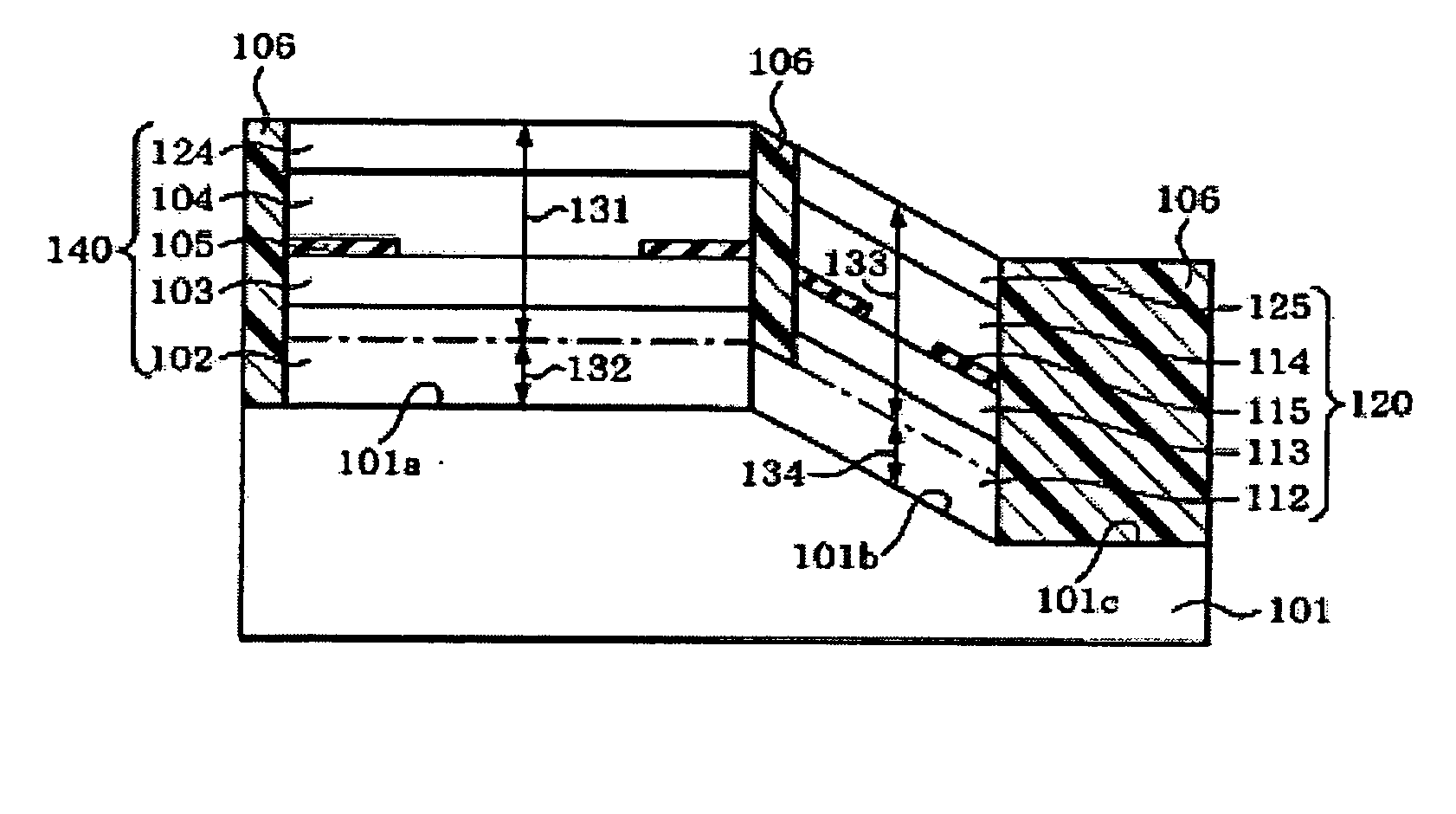
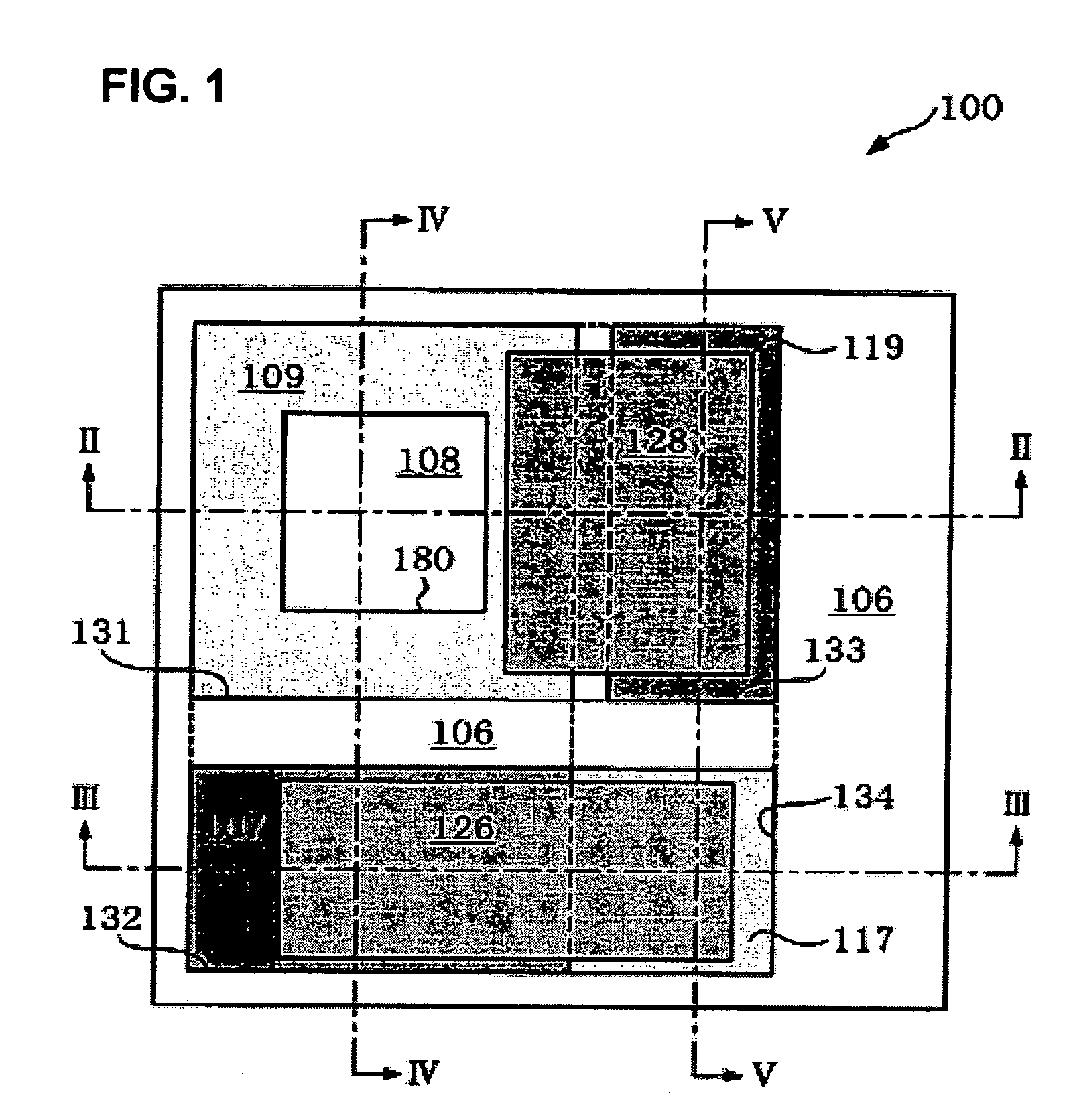
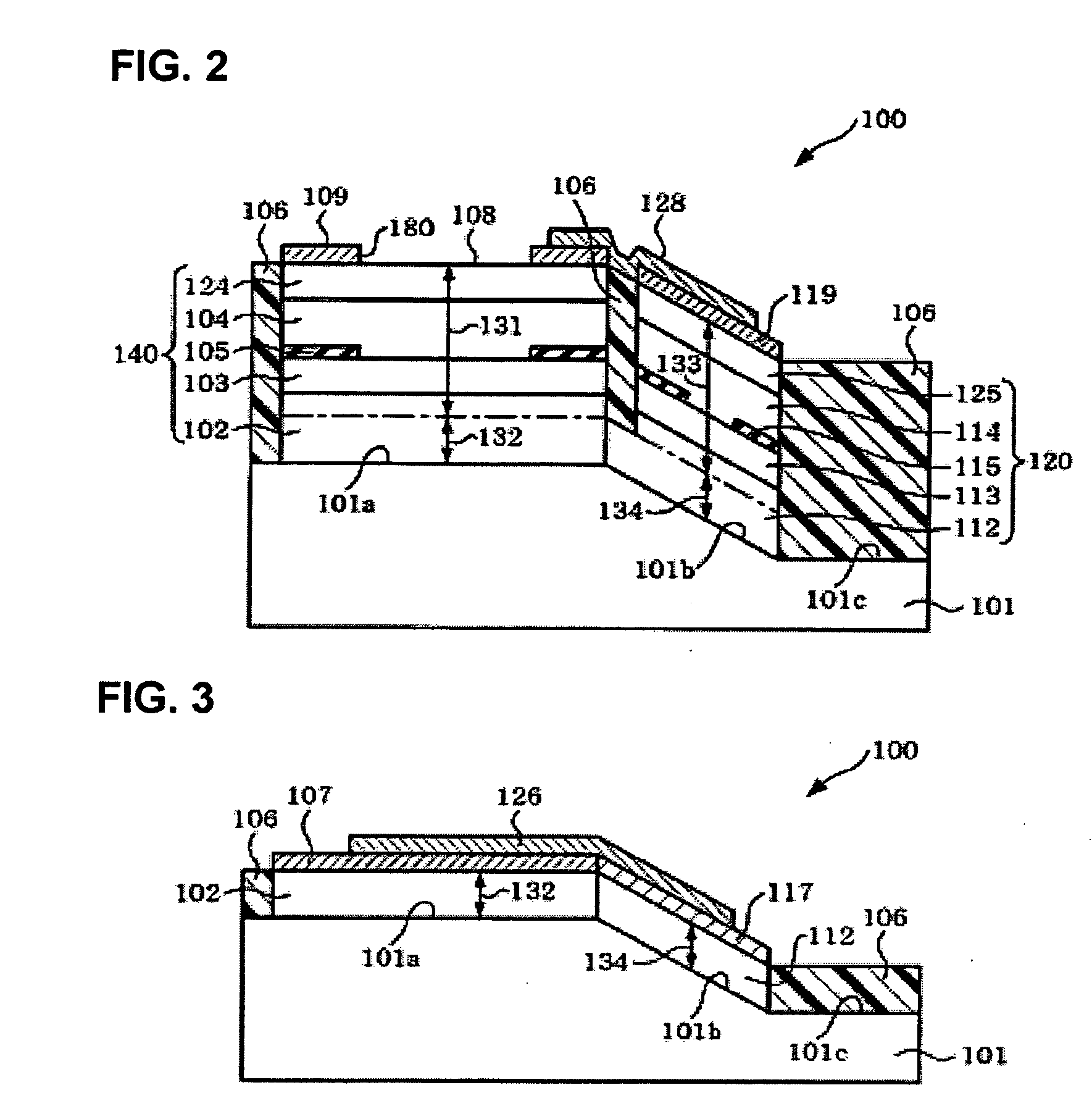
[0052]FIG. 1 is a plan view schematically showing the surface-emitting type device 100, FIG. 2 is a cross-sectional view taken along a line II-II of FIG. 1, FIG. 3 is a cross-sectional view taken along a line III-III of FIG. 1, FIG. 4 is a cross-sectional view taken along a line IV-IV of FIG. 1, FIG. 5 is a cross-sectional view taken along a line V-V of FIG. 1, and FIG. 6 is a circuit diagram of the surface-emitting type device 100.

[0053] The surface-emitting type device 100 includes, as shown in FIG. 2, FIG. 4 and FIG. 5, a substrate 101, an emission section 140 and a rectification section 120. The present embodiment is described as to a case where the emission section 140 functions as a surface-emitting type semiconductor laser, and the rectification section 120 functions a...


PUM


Abstract

A surface-emitting type device includes a substrate including a first face and a second face that is tilted with respect to the first face and has a plane index different from a plane index of the first face, an emission section formed above the first face, and a rectification section formed above the second face, wherein the emission section includes a first semiconductor layer of a first conductivity type, an active layer formed above the first semiconductor layer, and a second semiconductor layer of a second conductivity type formed above the active layer, the rectification section includes a first semiconductor layer of the second conductivity type, and a second semiconductor layer of the first conductivity type formed above the first semiconductor layer, the first semiconductor layer of the emission section and the first semiconductor layer of the rectification section are formed by a common process and include the same impurity, the emission section and the rectification section are electrically connected in parallel with each other, and the rectification section has a rectification action in a reverse direction with respect to the emission section.

Description

[0001] The entire disclosure of Japanese Patent Application No. 2005-079183, filed Mar. 18, 2005 is expressly incorporated by reference herein. BACKGROUND [0002] 1. Technical Field [0003] The present invention relates to surface-emitting type devices and methods for manufacturing the same. [0004] 2. Related Art [0005] A surface-emitting type semiconductor laser has a smaller device volume compared to an edge-emitting type semiconductor laser, such that the electrostatic breakdown voltage of the device itself is low. For this reason, the device may be damaged by static electricity caused by a machine or an operator in a mounting process. In particular, a surface-emitting type device such as a surface-emitting type semiconductor laser has a certain tolerance to a voltage in a forward direction, but has a low tolerance to a voltage in a reverse direction, and the device may be destroyed when a voltage in a reverse direction is impressed. A variety of measures are usually implemented in...

Claims


Application Information

Patent Timeline
Patent Type & Authority Applications(United States)
IPC IPC(8): H01L21/31H01L21/469H01L27/082H01L27/102H01L29/70H01L31/11
CPCH01L27/15H01S5/0207H01S5/0261H01S5/0425H01S5/06226H01S5/06825H01S5/18311H01S5/18338H01S5/3081H01S2301/176H01S5/04256H01S5/04257
Inventor ONISHI, HAJIMENISHIDA, TETSUO
Owner SEIKO EPSON CORP
Why Eureka
Try Eureka