
Systems and methods for reduced size detector electronics

a detector and electronic technology, applied in the field of medical imaging systems, can solve the problems of large number of signals, increased size and expense of associated electronics, and board-size limitations in z-assembly

Active Publication Date: 2017-03-30
GENERAL ELECTRIC CO
View PDF6 Cites 27 Cited by
  • Summary
  • Abstract
  • Description
  • Claims
  • Application Information

AI Technical Summary

Benefits of technology

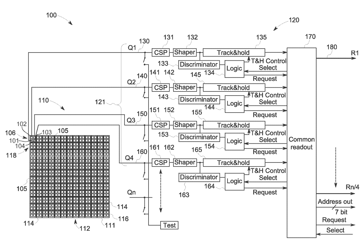
The patent text describes a radiation detector system that includes a pixelated detector and a processing assembly. The processing assembly has multiple input channels, a common readout, and a readout channel. Each input channel receives a signal from a pixel on the detector, and the common readout collects these signals. Each output signal has a unique address that identifies the input channel. The readout channel receives a readout output from the common readout, which contains signals from multiple input channels. The technical effects of this system include improved performance and efficiency in detecting and processing radiation signals, as well as reduced noise and improved accuracy in imaging and analysis applications.

Problems solved by technology

Use of a larger number of smaller pixels, however, results in a larger number of signals to be acquired and processed, increasing the size and expense of the associated electronics.
Such board-size limitations may occur in Z-assembly when an electronic board, including electronic-chips (e.g., Memories, FPGA's, or ASIC's), is attached directly, by interconnections, onto a semiconductor radiation-detector.
For example, as electronic chips, such as ASIC's, become larger to be able to process larger number of electronic-signals, stresses and strains due to thermal expansion between electronics and a substrate may result in increased failures of electronics.

Method used


Image

  • Systems and methods for reduced size detector electronics
  • Systems and methods for reduced size detector electronics
  • Systems and methods for reduced size detector electronics

Examples


Embodiment Construction

[0013]The foregoing summary, as well as the following detailed description of certain embodiments and claims, will be better understood when read in conjunction with the appended drawings. To the extent that the figures illustrate diagrams of the functional blocks of various embodiments, the functional blocks are not necessarily indicative of the division between hardware circuitry. Thus, for example, one or more of the functional blocks (e.g., processors, controllers or memories) may be implemented in a single piece of hardware (e.g., a general purpose signal processor or random access memory, hard disk, or the like) or multiple pieces of hardware. Similarly, the programs may be stand alone programs, may be incorporated as subroutines in an operating system, may be functions in an installed software package, and the like. It should be understood that the various embodiments are not limited to the arrangements and instrumentality shown in the drawings.

[0014]As used herein, the terms...


PUM


Abstract

A radiation detector processing assembly is provided including at least one application specific integrated circuit (ASIC). The radiation detector processing assembly includes plural input channels, a common readout, and a readout channel. Each input channel is configured to receive an input corresponding to a detection event from a pixel of a pixelated detector. The common readout is operably coupled to the plural input channels, and is configured to receive a corresponding output signal from each input channel. Each corresponding output signal has a unique address identifying the corresponding input channel. The readout channel is configured to receive a corresponding readout output from the common readout. The readout output includes output signals from a corresponding group of input channels.

Description

BACKGROUND[0001]The subject matter disclosed herein relates generally to medical imaging systems, and more particularly to radiation detection systems.[0002]In nuclear medicine (NM) imaging, such as single photon emission computed tomography (SPECT) or positron emission tomography (PET) imaging, radiopharmaceuticals are administered internally to a patient. Detectors (e.g., gamma cameras, X-Ray cameras, and detectors and cameras for ionizing radiation), typically installed on a gantry, capture the radiation emitted by the radiopharmaceuticals and this information is used, by a computer, to form images. The NM images primarily show physiological function of, for example, the patient or a portion of the patient being imaged. Smaller pixel sizes may be utilized to improve energy and / or spatial resolution. Use of a larger number of smaller pixels, however, results in a larger number of signals to be acquired and processed, increasing the size and expense of the associated electronics. A...

Claims


Application Information

Patent Timeline
Patent Type & Authority Applications(United States)
IPC IPC(8): G01T1/24G21K1/02H04N25/46
CPCG21K1/02G01T1/247G01T1/17H01L27/14605H01L27/146H04N25/46
Inventor SHAHAR, ARIEOFAN, AVISHAILEVY, JEFFREY MICHAELCOHEN-ERNER, MOSHEGLAZER, YARON
Owner GENERAL ELECTRIC CO
Learn More