Method for manufacturing display device and method for manufacturing electronic device

Active Publication Date: 2017-02-02
SEMICON ENERGY LAB CO LTD
View PDF2 Cites 11 Cited by
  • Summary
  • Abstract
  • Description
  • Claims
  • Application Information

AI Technical Summary

Benefits of technology

The present invention provides a method for manufacturing a display device that does not easily damage an electrode, resulting in a high yield of reliable and manufacturable display devices. The method also prevents signal attenuation, electric power attenuation, and display region damage due to increases in wiring resistance, providing a display device with high visibility, display quality, reliability, and low power consumption. Additionally, the invention provides a flexible display device with a reduced risk of breaking or low power consumption.

Problems solved by technology

However, a method in which part of a flexible substrate is removed by a laser beam or with an edged tool has a problem in that an electrode included in a display device is damaged easily and the reliability and manufacturing yield of the display device are reduced easily.

Method used


Image

  • Method for manufacturing display device and method for manufacturing electronic device
  • Method for manufacturing display device and method for manufacturing electronic device
  • Method for manufacturing display device and method for manufacturing electronic device

Examples


embodiment 1

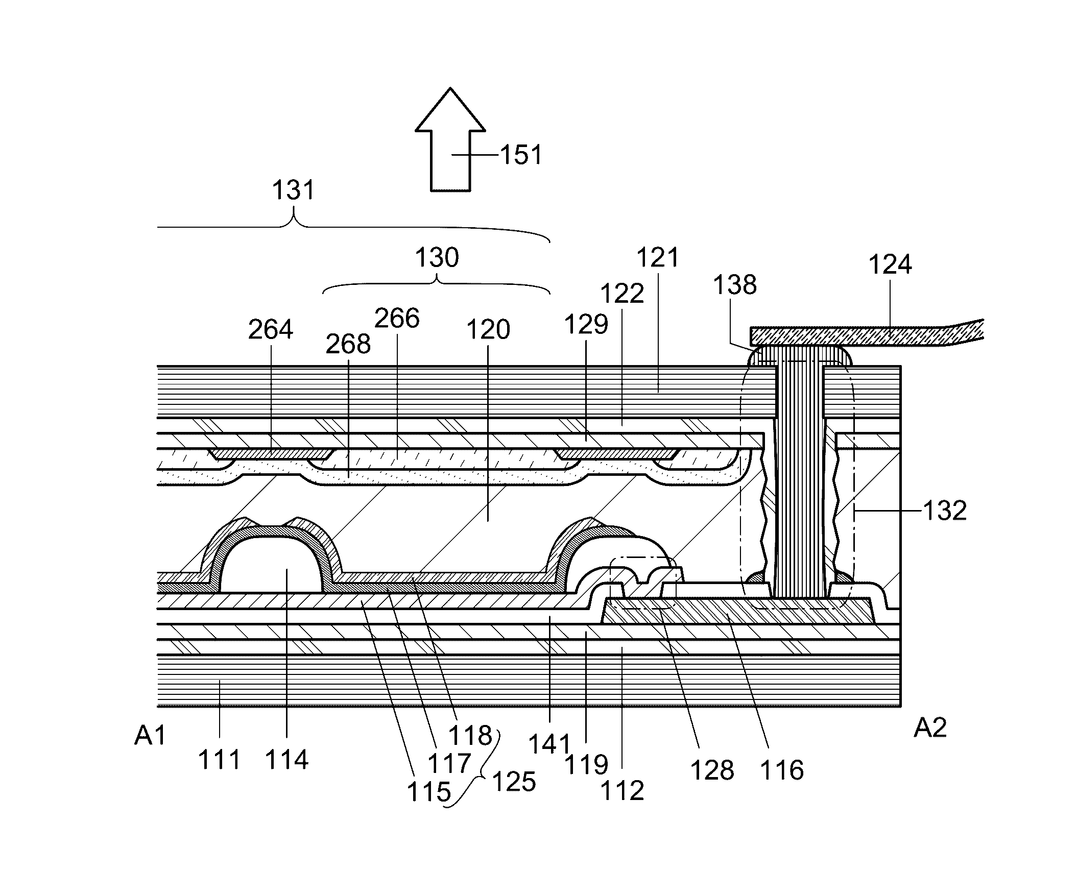
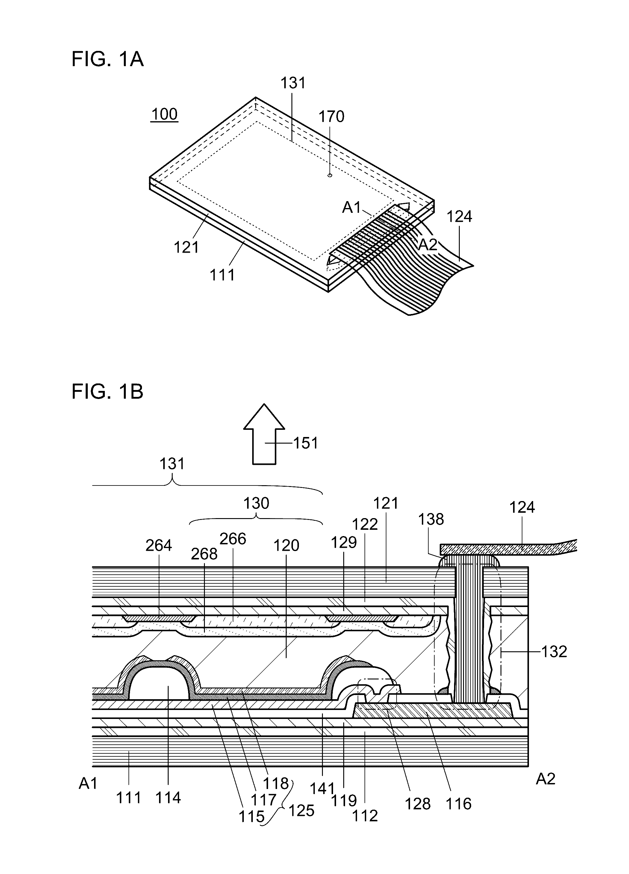
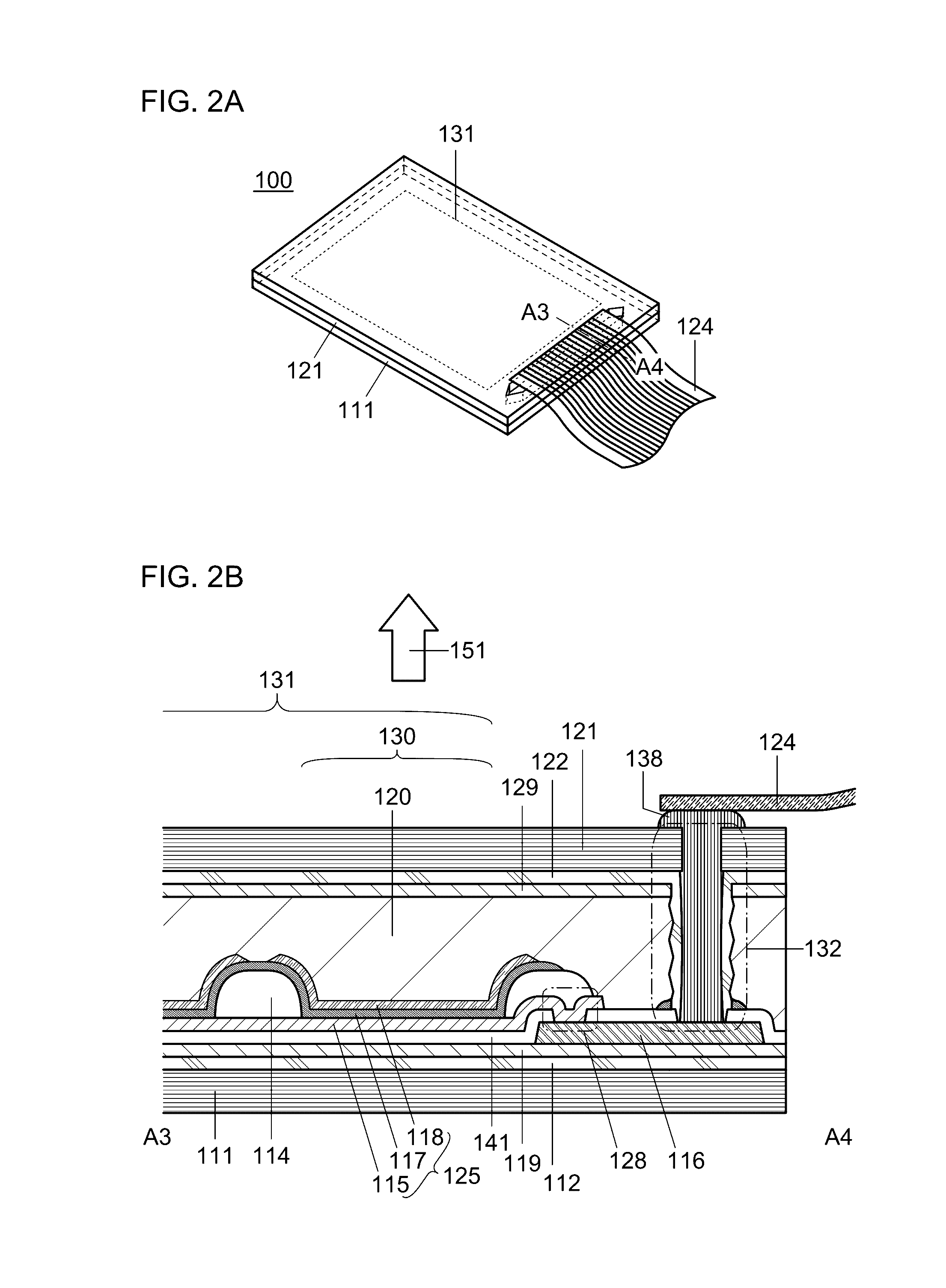
[0083]A structure example of a display device 100 of one embodiment of the present invention will be described with reference to FIGS. 1A and 1B, FIGS. 2A and 2B, FIGS. 3A and 3B, FIGS. 4A to 4E, FIGS. 5A to 5D, FIGS. 6A to 6F, FIGS. 7A to 7C, FIGS. 8A and 8B, FIGS. 9A and 9B, FIGS. 10A and 10B, FIGS. 11A and 11B, and FIGS. 12A and 12B. FIG. 1A is a perspective view of the display device 100 to which an external electrode 124 is connected, and FIG. 1B is a cross-sectional view taken along the dashed-dotted line A1-A2 in FIG. 1A. Note that the display device 100 disclosed in this specification is a display device in which a light-emitting element is used as a display element. As the display device 100 of one embodiment of the present invention, a display device having a top-emission structure is described as an example. Note that the display device 100 can be a display device having a bottom-emission structure or a dual-emission structure.

[0084]The display device 100 described in thi...

embodiment 2

[0187]In this embodiment, a display device 200 having a structure different from the structure of the display device 100 described in the above embodiment will be described with reference to FIGS. 18A and 18B. FIG. 18A is a perspective view of the display device 200, and FIG. 18B is a cross-sectional view taken along the dashed-dotted line A5-A6 in FIG. 18A.

[0188]The display device 200 described in this embodiment includes a display region 231 and a peripheral circuit 251. The display device 200 further includes the electrode 116 and the light-emitting element 125 including the electrode 115, the EL layer 117, and the electrode 118. A plurality of light-emitting elements 125 are formed in the display region 231. A transistor 232 for controlling the amount of light emitted from the light-emitting element 125 is connected to each light-emitting element 125.

[0189]The electrode 116 is electrically connected to the external electrode 124 through the anisotropic conductive connection laye...

embodiment 3

[0224]In this embodiment, a specific structure example of the display device 200 will be described with reference to FIGS. 21A to 21C and FIGS. 22A1 to 22B2.

[0225]FIG. 21A is a block diagram illustrating the structure of a display device 3100. The display device 3100 includes a display region 3131, a circuit 3132, and a circuit 3133. The circuit 3132 functions as a scan line driver circuit, for example. The circuit 3133 functions as a signal line driver circuit, for example.

[0226]The display device 3100 includes m scan lines 3135 which are arranged parallel or substantially parallel to each other and whose potentials are controlled by the circuit 3132, and n signal lines 3136 which are arranged parallel or substantially parallel to each other and whose potentials are controlled by the circuit 3133. The display region 3131 includes a plurality of pixels 3130 arranged in a matrix of m rows and n columns. Note that each of m and n is a natural number of 2 or more.

[0227]Each of the scan...


PUM


Abstract

Provided is a method for manufacturing a highly reliable display device. The method includes steps of providing a first layer, a first insulating layer, an electrode, and a second insulating layer over a first surface of a first substrate; removing a part of the second insulating layer to provide a first opening; providing a display element and a second layer over the second insulating layer; providing a third layer and a third insulating layer over a second surface of a second substrate; removing part of the third layer and part of the third insulating layer to provide a second opening; overlapping the first substrate and the second substrate with a bonding layer positioned therebetween such that the first surface and the second surface face each other and the first opening and the second opening have an overlap region; separating the first substrate and the first layer from the first insulating layer; providing a third substrate such that the first insulating layer and the third substrate overlap with each other; separating the second substrate, part of the bonding layer, part of the second layer, and the third layer from the third insulating layer; and providing a fourth substrate such that the third insulating layer and the fourth substrate overlap with each other.

Description

BACKGROUND OF THE INVENTION[0001]1. Field of the Invention[0002]The present invention relates to a display device. The present invention also relates to a method for manufacturing the display device.[0003]Note that one embodiment of the present invention is not limited to the above technical field.[0004]Note that in this specification and the like, a semiconductor device generally means a device that can function by utilizing semiconductor characteristics. Thus, a semiconductor element such as a transistor or a diode and a semiconductor circuit are semiconductor devices. A display device, a light-emitting device, a lighting device, an electro-optical device, an electronic device, and the like may include a semiconductor element or a semiconductor circuit. Therefore, a display device, a light-emitting device, a lighting device, an electro-optical device, an electronic device, and the like include a semiconductor device in some cases.[0005]2. Description of the Related Art[0006]In rec...

Claims


Application Information

Patent Timeline
IPC IPC(8): H01L51/00H01L51/56
CPCH01L51/003H01L51/0097H01L51/56H01L2227/323G02F1/134309H01L2251/5338H01L2251/5315G02F1/1368G02F1/136213H01L2227/326G02F1/133305G02F1/1345H01L29/78648H01L29/7869H01L29/78696H01L27/1225Y02E10/549G02F1/13613Y02P70/50H10K59/131H10K71/80H10K59/1201H10K2102/311H10K71/40H10K71/00H10K77/111
Inventor CHIDA, AKIHIRO
Owner SEMICON ENERGY LAB CO LTD
Why Eureka
Try Eureka