Controlling contamination particle trajectory from a beam-line electrostatic element

Active Publication Date: 2017-02-02
VARIAN SEMICON EQUIP ASSOC INC
View PDF6 Cites 15 Cited by
  • Summary
  • Abstract
  • Description
  • Claims
  • Application Information

AI Technical Summary

Benefits of technology

The patent describes a system and method for controlling the trajectory of particles in a beam-line component. A new electrostatic element is added to shape the local electrostatic field and prevent or limit the transport of particle defects along the ion beam-line. This allows for better control of particle movement using the shape of the beam-line electrostatic element.

Problems solved by technology

These residues build up on the beam-line components, causing spikes in the DC potentials during normal operation (e.g., in the case of electrically biased components) and eventually flake off, causing an increased likelihood of particulate contamination on the wafer.
Particulate contamination can result in device failure, poor film quality, changes in material resistivity, and impurity permeation.
Further, as device dimensions are reduced, tighter control of the etching profile translates to ever more stringent restrictions on the allowable particle contamination number, density and size.
This spike or hill of unreacted material may also degrade the device performance and reduce process yield.

Method used


Image

  • Controlling contamination particle trajectory from a beam-line electrostatic element
  • Controlling contamination particle trajectory from a beam-line electrostatic element
  • Controlling contamination particle trajectory from a beam-line electrostatic element

Examples


Embodiment Construction

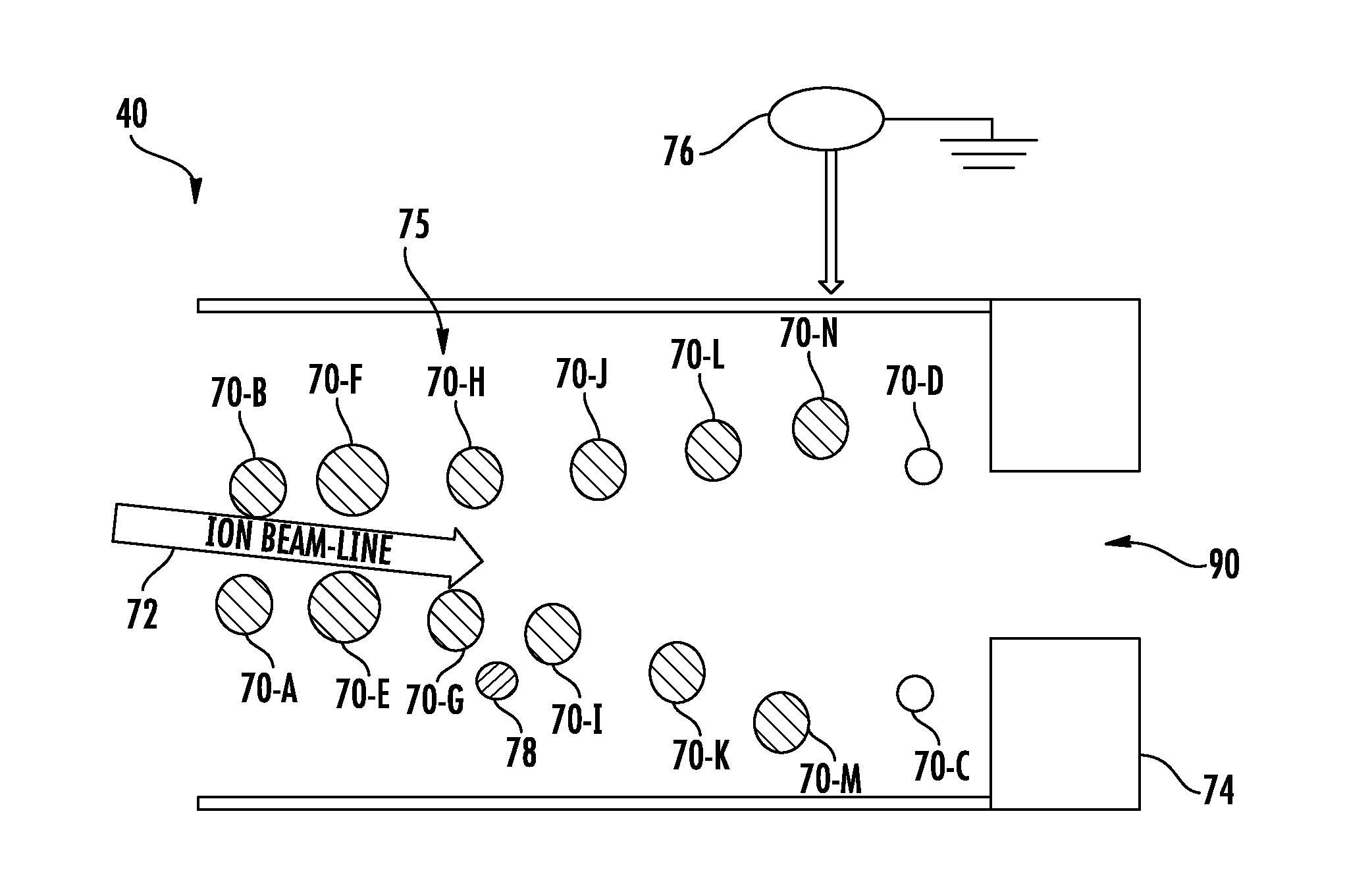
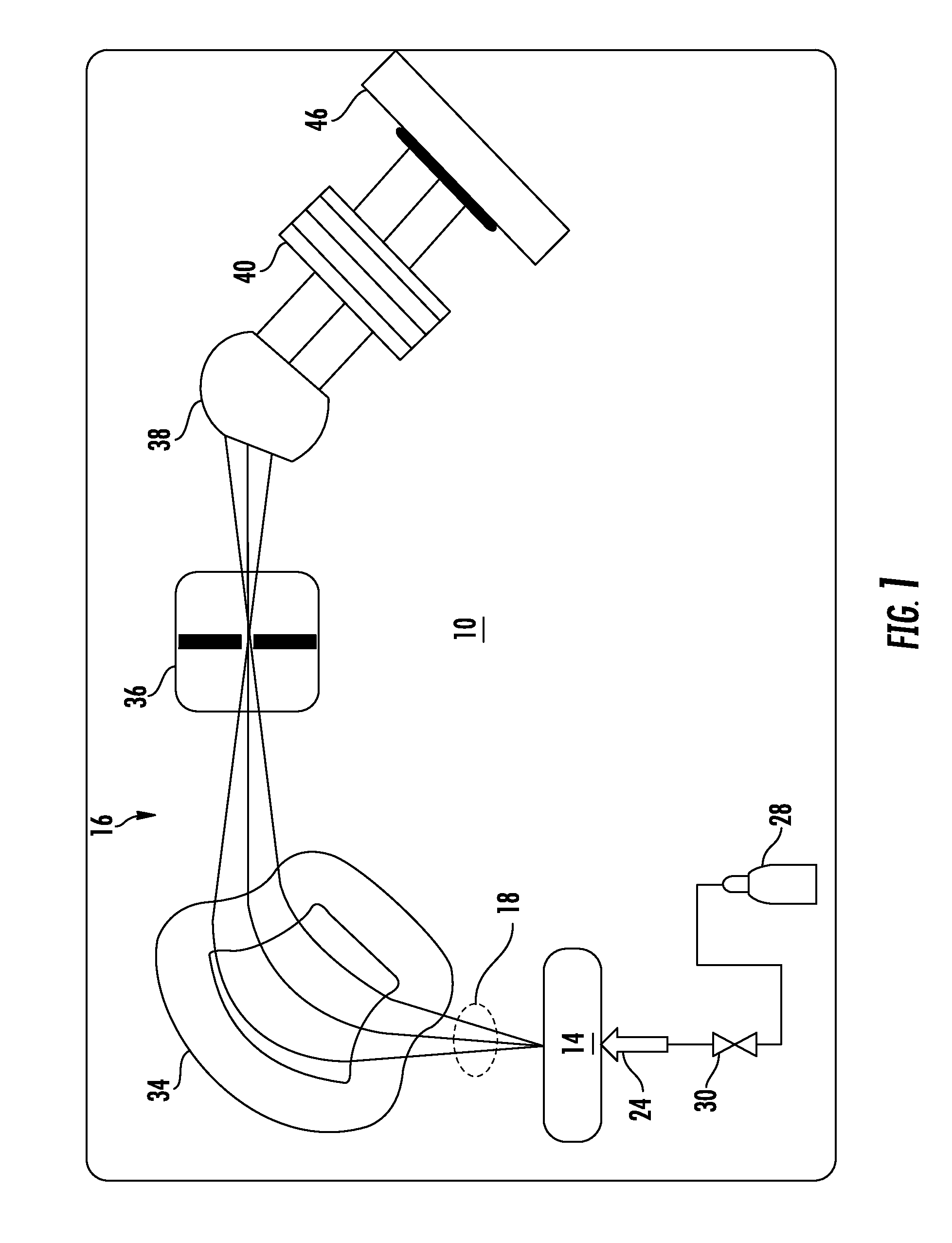
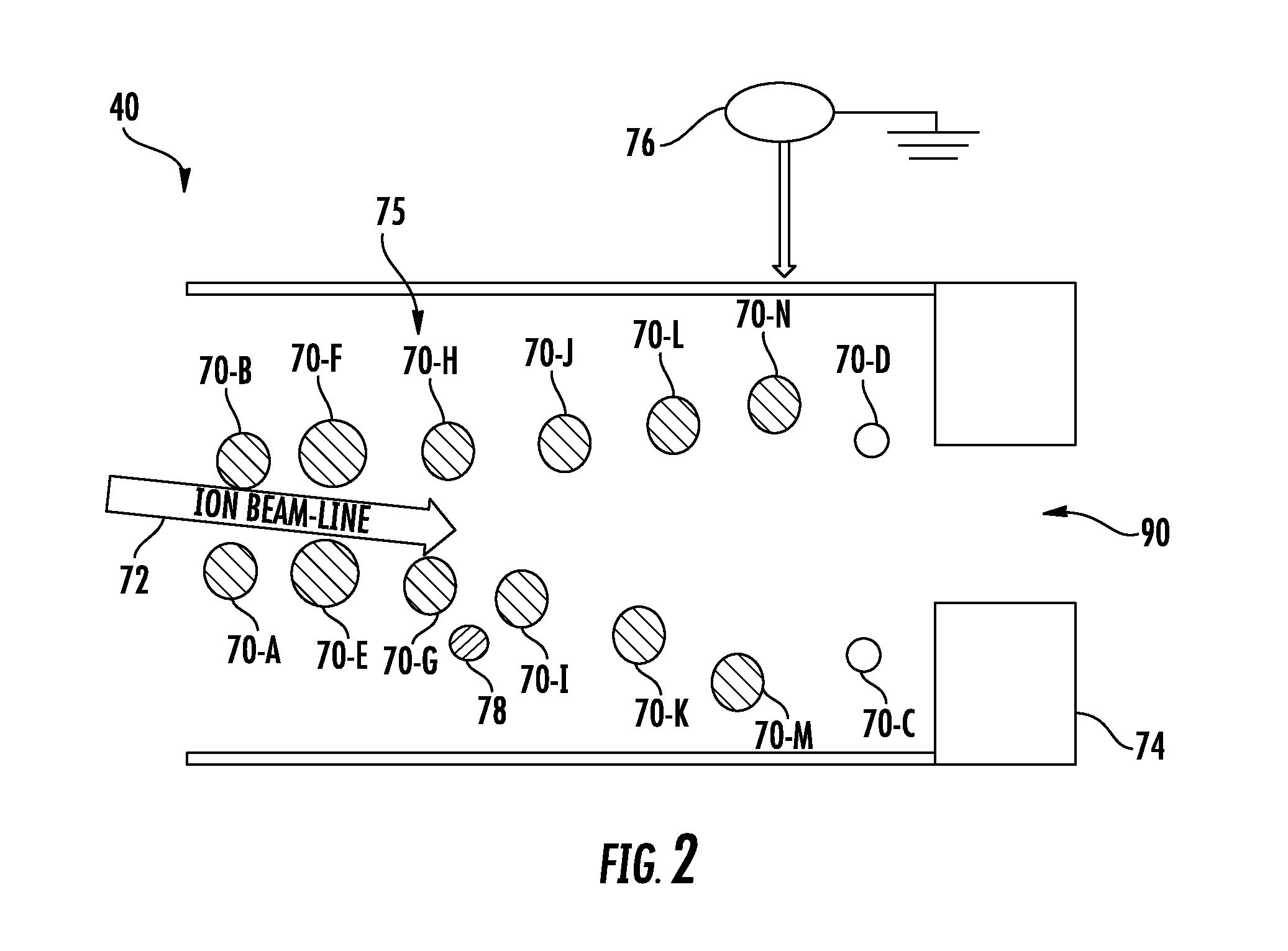
[0018]A system and method in accordance with the present disclosure will now be described more fully hereinafter with reference to the accompanying drawings, where embodiments of the system and method are shown. The system and method may be embodied in many different forms and are not to be construed as being limited to the embodiments set forth herein. Instead, these embodiments are provided so this disclosure will be thorough and complete, and will fully convey the scope of the system and method to those skilled in the art.

[0019]For the sake of convenience and clarity, terms such as “top,”“bottom,”“upper,”“lower,”“vertical,”“horizontal,”“lateral,” and “longitudinal” will be used herein to describe the relative placement and orientation of these components and their constituent parts, each with respect to the geometry and orientation of a component of a semiconductor manufacturing device as appearing in the figures. The terminology will include the words specifically mentioned, der...


PUM


Abstract

Provided herein are approaches for controlling particle trajectory from a beam-line electrostatic element. In an exemplary approach, a beam-line electrostatic element is disposed along a beam-line of an electrostatic filter (EF), and a voltage is supplied to the beam-line electrostatic element to generate an electrostatic field surrounding the beam-line electrostatic element, agitating a layer of contamination particles formed on the beam-line electrostatic element. A trajectory of a set of particles from the layer of contamination particles is then modified to direct the set of particles to a desired location within the EF. In one approach, the trajectory is controlled by providing an additional electrode adjacent the beam-line electrostatic element, and supplying a voltage to the additional electrode to control a local electrostatic field in proximity to the beam-line electrostatic element. In another approach, the trajectory is influenced by one or more geometric features of the beam-line electrostatic element.

Description

FIELD OF THE DISCLOSURE[0001]The disclosure relates generally to techniques for manufacturing electronic devices, and more particularly, to techniques for reducing particle contamination, generated within a process chamber, from reaching a wafer.BACKGROUND OF THE DISCLOSURE[0002]Ion implantation is a process of introducing dopants or impurities into a substrate via bombardment. In semiconductor manufacturing, the dopants are introduced to alter electrical, optical, or mechanical properties. For example, dopants may be introduced into an intrinsic semiconductor substrate to alter the type and level of conductivity of the substrate. In manufacturing an integrated circuit (IC), a precise doping profile provides improved IC performance. To achieve a desired doping profile, one or more dopants may be implanted in the form of ions in various doses and various energy levels.[0003]A conventional ion implantation system may comprise an ion source and a series of beam-line components. The ion...

Claims


Application Information

Patent Timeline
IPC IPC(8): H01J37/05H01J37/317H01J37/12
CPCH01J37/05H01J37/3171H01J37/12H01J2237/022H01J2237/028
Inventor LEE, WILLIAM DAVISLIKHANSKII, ALEXANDRE
Owner VARIAN SEMICON EQUIP ASSOC INC
Why Eureka
Try Eureka