
Repair information providing device in an integrated circuit

a technology of repair information and integrated circuit, which is applied in the field of semiconductor circuits, can solve the problems of increasing the storage space for the repair information and the loading time necessary to load the repair information, and the size of the repair information representing addresses, so as to reduce the size of storage space and reduce the loading tim

Active Publication Date: 2017-01-26
SAMSUNG ELECTRONICS CO LTD
View PDF3 Cites 7 Cited by
  • Summary
  • Abstract
  • Description
  • Claims
  • Application Information

AI Technical Summary

Benefits of technology

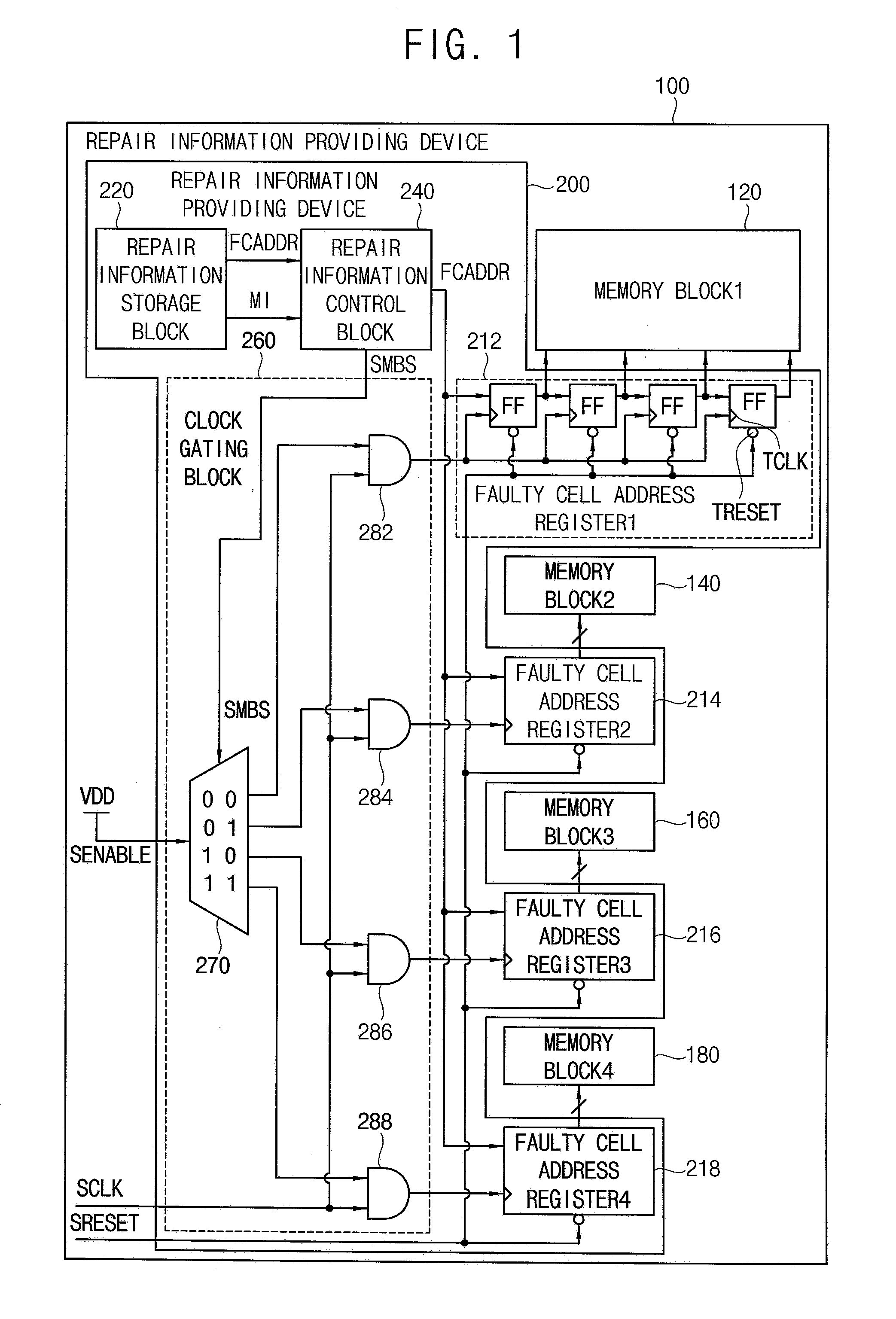
The patent text describes a device and integrated circuit that can provide repair information for a memory device. The device can include a repair information providing device and an integrated circuit that can reduce the amount of storage space needed and the time required to load the repair information. This is achieved by storing the address of the faulty cell and the memory index indicating the memory block with the faulty cell. The device can selectively provide the clock signal or the address of the faulty cell to the faulty cell address register connected to the memory block indicated by the memory index. This reduces the amount of storage space needed and the time required to load the repair information.

Problems solved by technology

However, as the number of the memory blocks included in the integrated circuit increases, a size of repair information representing addresses of faulty cells may increase, and thus storage space for the repair information and a loading time necessary to load the repair information may increase.

Method used


Image

  • Repair information providing device in an integrated circuit
  • Repair information providing device in an integrated circuit
  • Repair information providing device in an integrated circuit

Examples


Embodiment Construction

[0034]Exemplary embodiments will be described more fully with reference to the accompanying drawings, in which embodiments are shown. The inventive concept of the disclosure may, however, be embodied in many different forms and should not be construed as limited to the exemplary embodiments set forth herein. Rather, these exemplary embodiments are provided so that this disclosure will be thorough and complete, and will fully convey the scope of the disclosure to those skilled in the art Like reference numerals refer to like elements throughout this application.

[0035]It will be understood that, although the terms first, second, etc. may be used herein to describe various elements, these elements should not be limited by these terms. These terms are used to distinguish one element from another. For example, a first element could be termed a second element, and, similarly, a second element could be termed a first element, without departing from the scope of the inventive concept.

[0036]...


PUM


Abstract

A repair information providing device in an integrated circuit including a plurality of memory blocks includes a plurality of faulty cell address registers connected to the memory blocks, respectively, a repair information storage block configured to store repair information including an address of a faulty cell and a memory index indicating a memory block having the faulty cell, a repair information control block configured to read the repair information from the repair information storage block, transfer the address of the faulty cell included in the repair information to the respective faulty cell address registers, and generate a memory block selection signal based on the memory index included in the repair information, and a clock gating block configured to receive a clock signal, and selectively transfer the clock signal to one of the faulty cell address registers connected to the memory block having the faulty cell in response to receiving the memory block selection signal.

Description

CROSS-REFERENCE TO RELATED APPLICATION[0001]This U.S. non-provisional application claims priority under 35 U.S.C. §119 to Korean Patent Application No. 10-2015-0104097 filed on Jul. 23, 2015, in the Korean Intellectual Property Office (KIPO), the disclosure which is incorporated by reference herein in its entirety.BACKGROUND[0002]1. Field[0003]Methods and apparatuses consistent with exemplary embodiments relate to semiconductor circuits, more particularly, to repair information providing devices in integrated circuits.[0004]2. Description of the Related Art[0005]An integrated circuit, such as a system-on-chip (SoC), may include a plurality of embedded memory blocks. When a faulty cell is detected during a testing process for testing the embedded memory blocks of the SoC, the faulty cell of the memory block may be replaced with a redundancy cell in the memory block. As a result, the integrated circuit including the memory block having the faulty cell need not be discarded.[0006]Accor...

Claims


Application Information

Patent Timeline
IPC IPC(8): G06F11/07
CPCG06F11/0793G06F11/0751G06F11/0727G06F11/073
Inventor HAN, JU-HEELIM, YO-SEOPHAN, DONG-KWAN
Owner SAMSUNG ELECTRONICS CO LTD
Learn More