
Apparatus and method for removing particles present on a wafer using photoelectrons and an electric field

Active Publication Date: 2016-11-17
SK HYNIX INC
View PDF6 Cites 2 Cited by
  • Summary
  • Abstract
  • Description
  • Claims
  • Application Information

AI Technical Summary

Benefits of technology

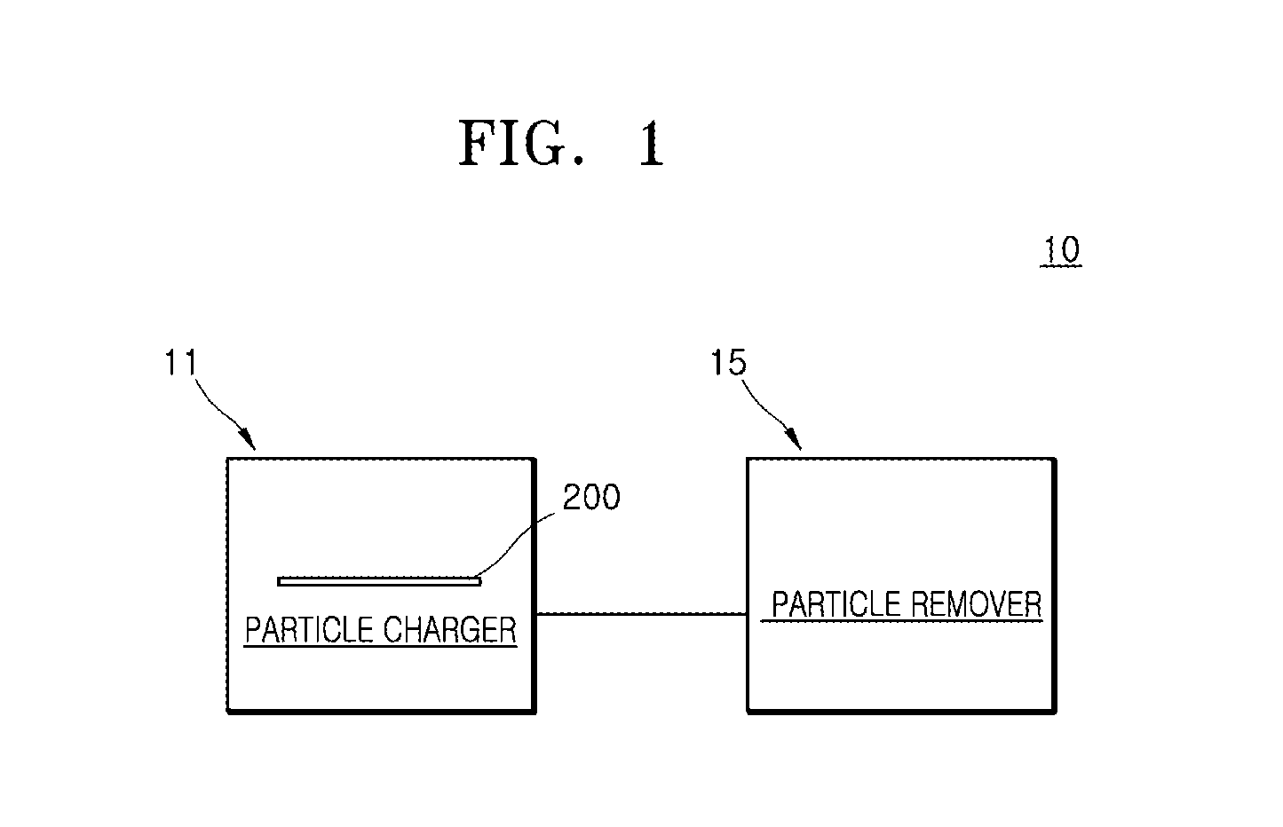
The patent describes an apparatus and method for removing particles from a wafer by using photoelectrons and an electric field. The apparatus includes a particle charger for charging the particles, a particle remover for detaching the charged particles from the wafer, and a wafer processing unit for performing a wafer process. The technical effects include improved wafer quality and reduced particle contamination during the manufacturing process.

Problems solved by technology

Contaminants such as particles present on or adsorbed onto a surface of the wafer may cause process failures.
Particles present on or adsorbed onto a wafer may cause process defects, and thus a process yield may be reduced.
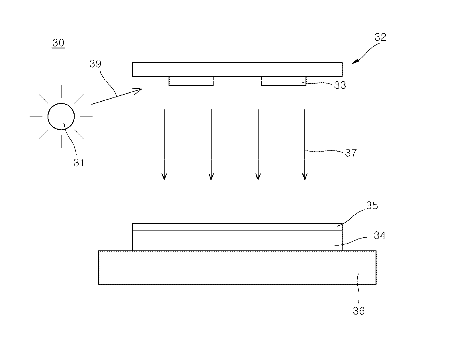
For example, if a patterning process is performed on a material layer that is formed on the front-side surface of the wafer whose back-side surface is contaminated with particles, non-uniform patterns may be formed on the front-side surface of the wafer because of a sloped profile of the front-side surface of the wafer due to the particles.
This may cause a defocus phenomenon.
The defocus phenomenon may lead to a non-uniform exposure step.
As a result, the uniformity of patterns formed on the front-side surface of the wafer may be degraded.
Accordingly, a lot of effort has been introduced to remove particles adsorbed onto a back-side surface of a wafer prior to performing a wafer-processing process, such as an exposure step of a lithography process.

Method used


Image

  • Apparatus and method for removing particles present on a wafer using photoelectrons and an electric field
  • Apparatus and method for removing particles present on a wafer using photoelectrons and an electric field
  • Apparatus and method for removing particles present on a wafer using photoelectrons and an electric field

Examples


Embodiment Construction

[0020]The terms used in the following embodiments may be terms which are selected with consideration of their functions in the embodiments, and the meanings of the terms may be different according to the user's intention or the customs in the art. The terms used herein should be interpreted as being defined if the terms are defined in the specification. Unless otherwise defined, all terms (including technical and scientific terms) used herein have the same meaning as commonly understood by one of ordinary skill in the art to which the present disclosure belongs.

[0021]It will be understood that although the terms first, second, third etc. may be used herein to describe various elements, these elements should not be limited by these terms. These terms are only used to distinguish one element from another element. Thus, a first element in some embodiments could be termed a second element in other embodiments without departing from the teachings of the present disclosure.

[0022]Same refe...


PUM


Abstract

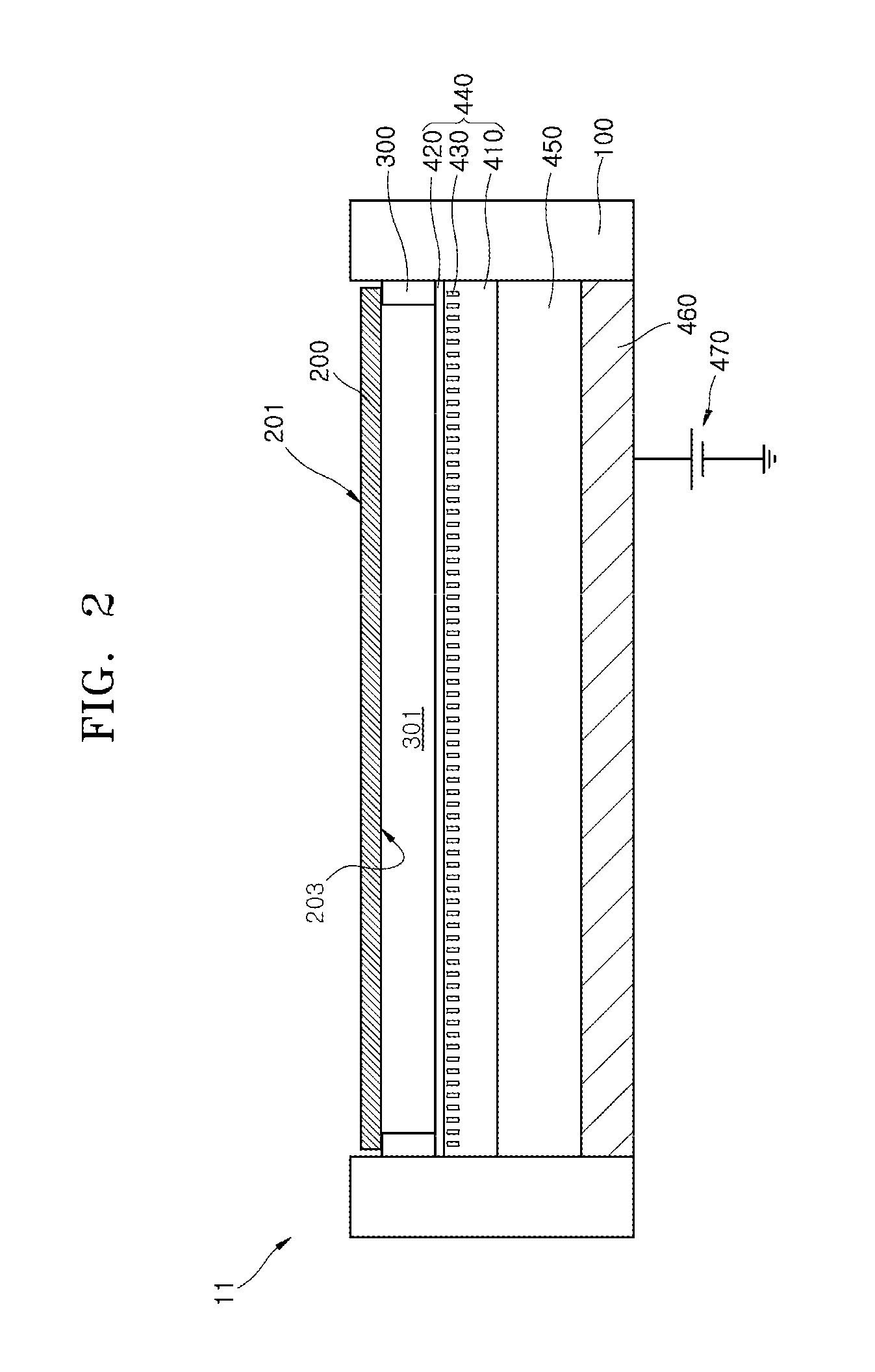
A wafer processing apparatus includes a particle charger for charging particles adsorbed onto a wafer with photoelectrons emitted from an emitter metal layer and a particle remover for applying an electric field to the wafer, which removes the charged particles from the wafer.

Description

CROSS-REFERENCE TO RELATED APPLICATION[0001]The present application claims priority under 35 U.S.C 119(a) to Korean Patent Application No. 10-2015-0067525, filed on May 14, 2015, in the Korean Intellectual Property Office, which is incorporated herein by reference in its entirety as set forth in full.BACKGROUND[0002]1. Technical Field[0003]Various embodiments of the present disclosure relate to semiconductor technologies and, more particularly, to an apparatus and method for removing particles present on a wafer using photoelectrons and an electric field.[0004]2. Related Art[0005]Semiconductor technologies may include processes for forming patterns on a substrate or a wafer to integrate electronic circuits. Contaminants such as particles present on or adsorbed onto a surface of the wafer may cause process failures. Thus, the particles adsorbed onto the surface of the wafer have to be removed in order to form uniform patterns having desired features throughout the wafer.[0006]Particl...

Claims


Application Information

Patent Timeline
IPC IPC(8): H01L21/322B08B6/00
CPCB08B6/00H01L21/3221H01L21/02057H01L21/0209H01L21/67028
Inventor SIM, JAE HEEKIM, SI HYUN
Owner SK HYNIX INC
Learn More