
Optical Metrology With Small Illumination Spot Size

a technology of optical metrology and spot size, applied in the field of optical metrology with small illumination spot size, can solve the problems of undesirable enlargement of the measurement box size at large aois, difficult to preserve a small measurement box size, and difficult to achieve desired box size specification

Active Publication Date: 2016-11-17
KLA CORP
View PDF14 Cites 15 Cited by
  • Summary
  • Abstract
  • Description
  • Claims
  • Application Information

AI Technical Summary

Benefits of technology

The patent describes a system for measuring the wavefront of a light beam. The system includes an illumination source, a spatial light modulator, and a wavefront sensor. The spatial light modulator is located in the illumination path and can adjust the amplitude and phase distribution of the light beam to reduce wavefront errors and shape the beam. The system also includes an illumination aperture that is tilted at an oblique angle to overcome defocusing effects. The technical effects of this system include improved accuracy in measuring wavefront errors and cancellation of contamination signals.

Problems solved by technology

However, it remains a challenge to preserve a small measurement box size.
In the semiconductor industry, where wafer space allocated to metrology targets is limited (often, within the scribe line or even within die), the desired box size specification can be often very challenging, such as 30 μm×30 μm, 10 μm×10 μm, or even smaller.
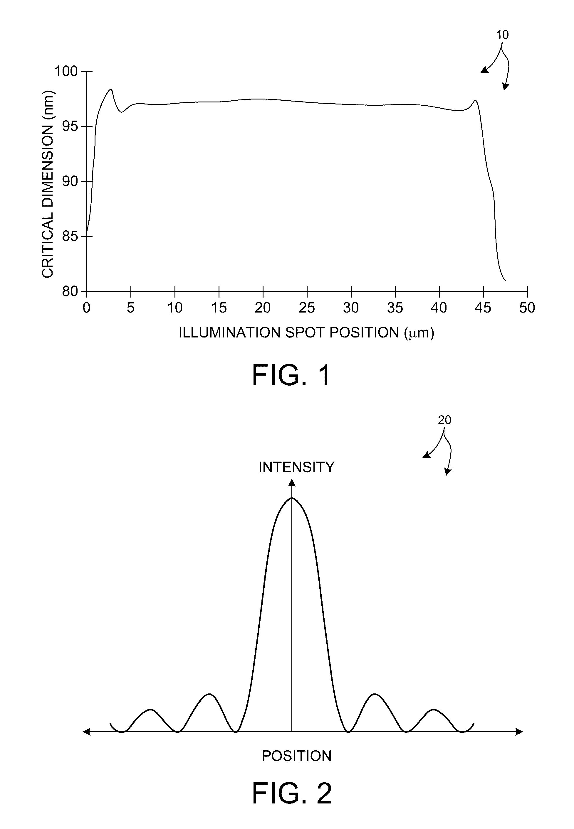
However, in some examples, e.g., in composition measurements where it is desirable to perform measurements at oblique, near-Brewster angles of incidence (AOI), geometric scaling effects cause an undesirable enlargement of the measurement box size at large AOIs.
Although increasing the NA addresses diffraction induced spillover, increasing the NA increases aberrations, increases cost, creates optical alignment difficulties, and reduces the transmission efficiency of the optical system.
Although reducing the size of the illumination aperture addresses geometrical properties of the spot image, the reduction in size of the illumination aperture increases coherence effects, reduces light throughput, and requires a tightening of optical system tolerances.
Despite existing approaches designed to control measurement box size, achieving a small measurement box size specification over the full measurement range is very challenging.
This is especially the case at both large oblique angles of incidence (AOI), where the incident beam covers a larger area, and at longer wavelengths, where diffraction effects introduce significant limitations.
As lithographic and inspection systems are pressed to higher resolutions, measurement box size becomes a limiting factor in maintaining device yield.
However, wavefront errors induced by the specimen itself and the collection optics are not visible in the wavefront measurement when the wavefront sensor is located in the illumination path.

Method used


Image

  • Optical Metrology With Small Illumination Spot Size
  • Optical Metrology With Small Illumination Spot Size
  • Optical Metrology With Small Illumination Spot Size

Examples


Embodiment Construction

[0056]Reference will now be made in detail to background examples and some embodiments of the invention, examples of which are illustrated in the accompanying drawings.

[0057]Methods and systems for tailoring the illumination provided to a specimen in specific measurement applications are described herein. The illumination may be tailored to reduce the illumination spot size projected onto a measurement target and associated spillover onto area surrounding a measurement target. In another example, the illumination may be tailored to simplify optical design and alignment procedures. In yet another example, the illumination may be tailored to compensate for tool to tool variation. In some examples, a small illumination spot size may enable the use of a broad range of wavelengths and angles of incidence without having to expand the size of the measurement box. A smaller measurement box enables smaller metrology target sizes in many applications, thus preserving valuable wafer area. In s...


PUM

PropertyMeasurementUnit
sizeaaaaaaaaaa
sizeaaaaaaaaaa
sizeaaaaaaaaaa

Abstract

Methods and systems are presented to reduce the illumination spot size projected onto a measurement target and associated spillover onto area surrounding a measurement target. In one aspect, a spatial light modulator (SLM) is located in the illumination path between the illumination light source and the measurement sample. The SLM is configured to modulate amplitude, phase, or both, across the path of the illumination light to reduce wavefront errors. In some embodiments, the desired state of the SLM is based on wavefront measurements performed in an optical path of the metrology system. In another aspect, an illumination aperture having an image plane tilted at an oblique angle with respect to a beam of illumination light is employed to overcome defocusing effects in metrology systems that employ oblique illumination of the measurement sample. In some embodiments, the illumination aperture, objective lens, and specimen are aligned to satisfy the Scheimpflug condition.

Description

TECHNICAL FIELD[0001]The described embodiments relate to metrology systems and methods, and more particularly to methods and systems for improved measurement resolution with smaller measurement box sizes.BACKGROUND INFORMATION[0002]Semiconductor devices such as logic and memory devices are typically fabricated by a sequence of processing steps applied to a specimen. The various features and multiple structural levels of the semiconductor devices are formed by these processing steps. For example, lithography among others is one semiconductor fabrication process that involves generating a pattern on a semiconductor wafer. Additional examples of semiconductor fabrication processes include, but are not limited to, chemical-mechanical polishing, etch, deposition, and ion implantation. Multiple semiconductor devices may be fabricated on a single semiconductor wafer and then separated into individual semiconductor devices.[0003]A lithographic process, as described above, is performed to se...

Claims


Application Information

Patent Timeline
Patent Type & Authority Applications(United States)
IPC IPC(8): G01N21/21
CPCG01N21/211G01N2201/08G01N2021/213G01N21/956G01B2210/56G03F7/70625G01B11/24G01N21/8806G06F3/041
Inventor SAPIENS, NOAMPETERLINZ, KEVIN A.BUETTNER, ALEXANDERPURRUCKER, KERSTINSHCHEGROV, ANDREI V.
Owner KLA CORP
Learn More