Organic Light Emitting Display Device
- Summary
- Abstract
- Description
- Claims
- Application Information
AI Technical Summary
Benefits of technology
Problems solved by technology
Method used
Image
Examples
first embodiment
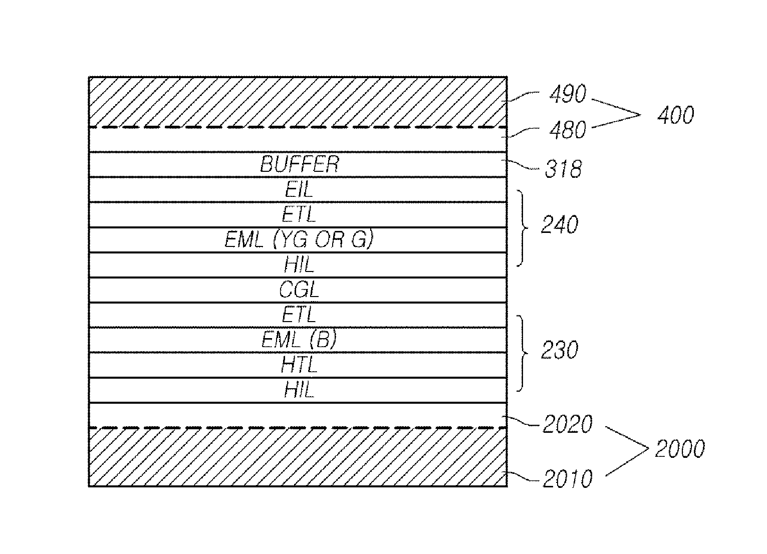
[0074]An example in which the compensation layer 480 and the electrode layer 490 are differentiated is described as the present invention. The compensation layer 480 may include two or more different layers according to the distribution or the composition ratio of the compensation material.
[0075]FIGS. 7 to 10 are cross-sectional views of a display panel according to the first embodiment of the present invention. For the convenience of description, the EIL to first electrode 210 below the buffer layer 318 is not shown.
[0076]FIG. 7 illustrates a configuration 411 in which a compensation material is not included in the electrode layer 490a according to the first embodiment of the present invention, and a configuration 412 in which the composition ratios of the compensation material in the compensation layer and the electrode layer are different.
[0077]In FIG. 7, one Cath_Comp may be deposited during a sputtering method in a process of forming second electrodes 400a and 400b. The Cath_Co...
second embodiment
[0096]FIG. 14 is a cross-sectional view of a display panel according to the present invention. For the convenience of description, the EIL to the first electrode 210 below the buffer layer 318 are not shown. In order to show the composition ratio or the distribution of the Rep_Comp, a molecule forming the Rep_Comp is shown as a reference numeral 1410. In the second electrode 1490, the composition ratio of the Rep_Comp 1410 is high in an area of an interface 1490a making contact with the buffer layer 318, and the composition ratio of the Rep_Comp 1410 is low in an area of an interface 1490b spaced apart from and far from the buffer layer 318. Therefore, a high resistance film is formed in the area close to the buffer layer 318 and thus a function of the compensation layer is provided to the area close to the buffer layer 318, and a low resistance film is formed in the area far from the buffer layer 318, and thus a function of the electrode layer is provided to the area far from the b...
third embodiment
[0098]As the present invention, the compensation layer may be formed using at least two types of Rep_Comp materials. For example, the compensation layer may be formed using Rep_Comp1 and Rep_Comp2 to increase a performance of a foreign body compensation. The Rep_Comp1 may be deposited together with the Cath_Comp to form the high resistance film. The Rep_Comp2 may be deposited together with the Cath_Comp to form the low resistance film of which a resistance is lower than that of the Rep_Comp1.
[0099]FIG. 18 is a cross-sectional view of a display panel according to the third embodiment of the present invention. A reference numeral 1801 is an embodiment in which two types of compensation materials form a second electrode 1800a including two layers of compensation layers 1881 and 1882 and the electrode layer 490. The Rep_Comp1 forms a resistance film of which a resistance is higher than that of the Rep_Comp2. A reference numeral 1802 is an embodiment in which three types of compensation ...
PUM
 Abstract
Description
Claims
Application Information
 - R&D
- Intellectual Property
- Life Sciences
- Materials
- Tech Scout
- Unparalleled Data Quality
- Higher Quality Content
- 60% Fewer Hallucinations
Browse by: Latest US Patents, China's latest patents, Technical Efficacy Thesaurus, Application Domain, Technology Topic, Popular Technical Reports.
© 2025 PatSnap. All rights reserved.Legal|Privacy policy|Modern Slavery Act Transparency Statement|Sitemap|About US| Contact US: help@patsnap.com


