
Semiconductor devices and methods of manufacturing the same

a technology of semiconductors and semiconductors, applied in the direction of semiconductor devices, electrical equipment, transistors, etc., can solve the problem that the dummy gate electrode may not work properly

Active Publication Date: 2016-10-20
SAMSUNG ELECTRONICS CO LTD
View PDF3 Cites 16 Cited by
  • Summary
  • Abstract
  • Description
  • Claims
  • Application Information

AI Technical Summary

Benefits of technology

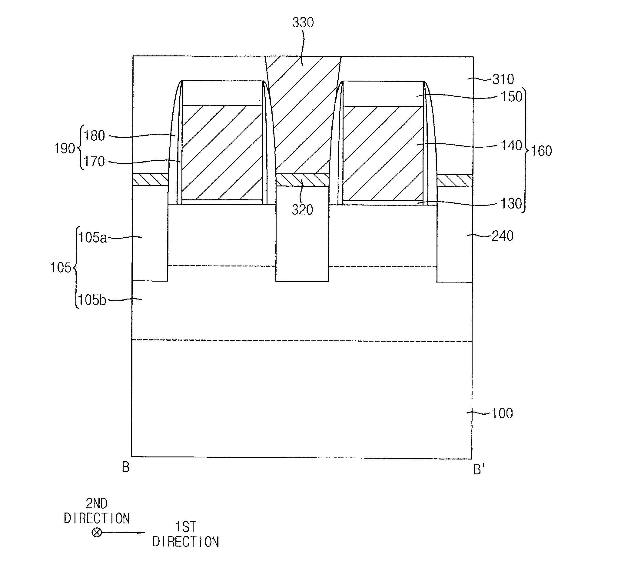
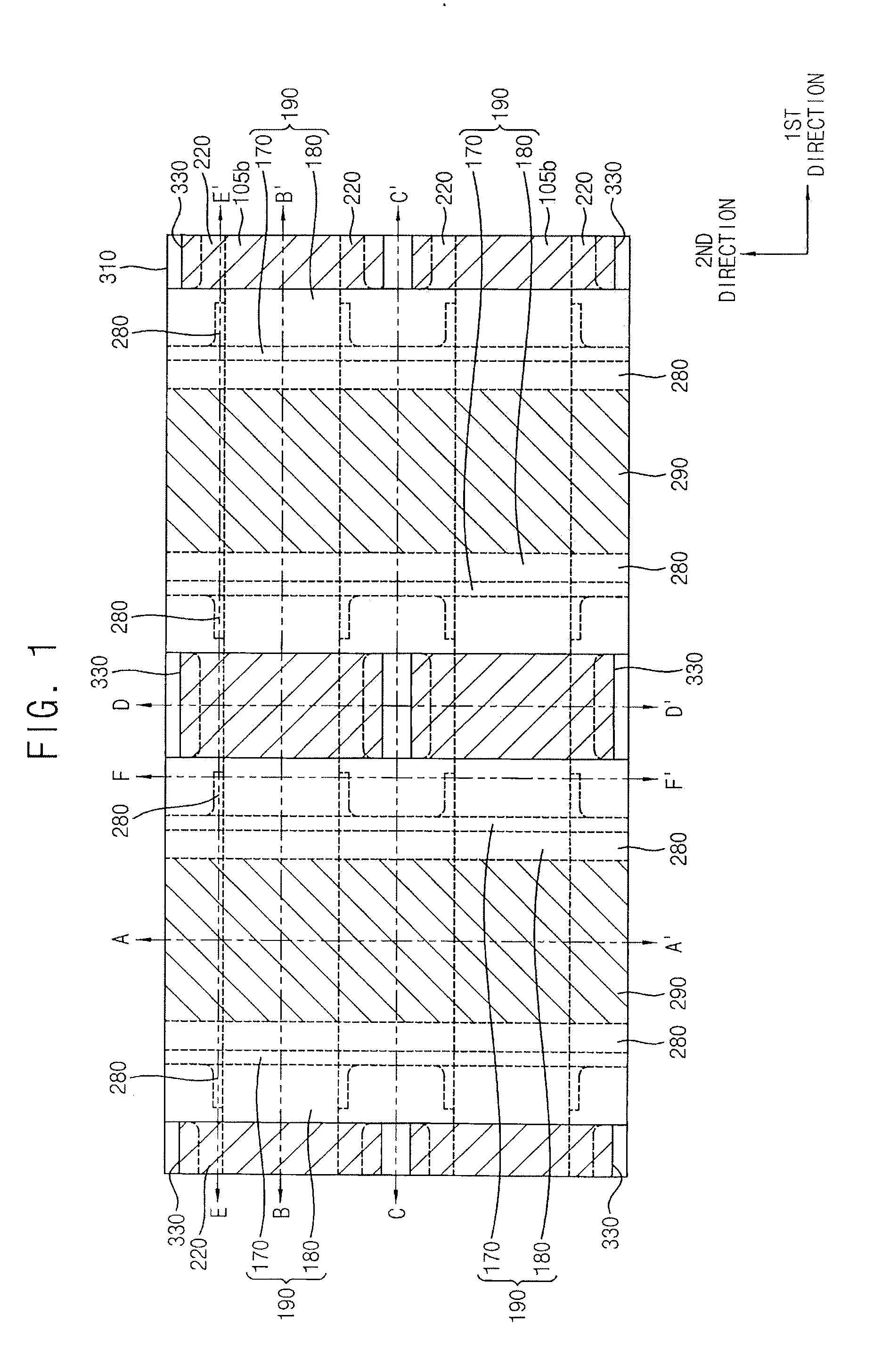
The patent describes a semiconductor device with a unique structure. The device includes active fins that protrude from an isolation layer on a substrate and extend in a first direction. There are also gate structures on the active fins that extend in a second direction perpendicular to the first direction. The sidewall of the first portion of the gate structures has a slope that is different from the slope of the second portion of the gate structures. The device also includes a spacer structure covering the sidewall of each gate structure and the sidewall of each active fin. The technical effects of this structure include improved performance and stability of the semiconductor device.

Problems solved by technology

This is because the lower portion of the dummy gate electrode may not be etched well, and thus may be exposed when a gate spacer is subsequently formed.

Method used


Image

  • Semiconductor devices and methods of manufacturing the same
  • Semiconductor devices and methods of manufacturing the same
  • Semiconductor devices and methods of manufacturing the same

Examples


Embodiment Construction

[0040]Example embodiments will now be described more fully hereinafter with reference to the accompanying drawings; however, they may be embodied in different forms and should not be construed as limited to the embodiments set forth herein. Rather, these embodiments are provided so that this disclosure will be thorough and complete, and will fully convey exemplary implementations to those skilled in the art. The embodiments may be combined to form additional embodiments.

[0041]It will also be understood that when a layer or element is referred to as being “on” another layer or substrate, it can be directly on the other layer or substrate, or intervening layers may also be present. Further, it will be understood that when a layer is referred to as being “under” another layer, it can be directly under, and one or more intervening layers may also be present. In addition, it will also be understood that when a layer is referred to as being “between” two layers, it can be the only layer b...


PUM


Abstract

A semiconductor device includes a plurality of active fins defined by an isolation layer on a substrate, a gate structure on the active fins and the isolation layer, and a gate spacer structure covering a sidewall of the gate structure. A sidewall of the gate structure includes first, second, and third regions having first, second, and third slopes, respectively. The second slope increases from a bottom toward a top of the second region. The second slope has a value at the bottom of the second region less than the first slope. The third slope is greater than the second slope.

Description

CROSS-REFERENCE TO RELATED APPLICATION[0001]Korean Patent Application No. 10-2015-0052408, filed on Apr. 14, 2015, and entitled, “Semiconductor Devices and Methods of Manufacturing the Same,” is incorporated by reference herein in its entirety.BACKGROUND[0002]1. Field[0003]One or more embodiments described herein relate to semiconductor devices and methods of manufacturing the semiconductor devices.[0004]2. Description of the Related Art[0005]A fin-type field effect transistor (finFET) may be manufactured by forming a dummy gate electrode to cross over active fins. As the distance between the active fins decreases, the dummy gate electrode may have a skirt-like shape. This is because the lower portion of the dummy gate electrode may not be etched well, and thus may be exposed when a gate spacer is subsequently formed. Consequently, a short may form between a gate electrode and a source / drain layer of the transistor.SUMMARY[0006]In accordance with one or more embodiments, a semicondu...

Claims


Application Information

Patent Timeline
Patent Type & Authority Applications(United States)
IPC IPC(8): H01L27/12H01L29/06H01L27/088
CPCH01L27/1211H01L29/0657H01L27/0886H01L29/0653H01L29/1033H01L29/42356H01L29/785H01L21/823431H01L21/823468
Inventor LEE, JUNG-HANLEE, JAE-HWANKIM, SANG-SUCHOI, HWAN-WOOKLEE, TAE-JONGHA, SEUNG-MO
Owner SAMSUNG ELECTRONICS CO LTD
Learn More