Wafer storage container

a storage container and wafer technology, applied in the direction of basic electric elements, semiconductor/solid-state device manufacturing, electric apparatus, etc., can solve the problems of uneven gas flow inside the wafer mounting area, the degradation of the reliability of the product, etc., and achieve the effect of efficient removal, smooth exhaustion and efficient removal

Active Publication Date: 2016-09-29
PICO & TERA CO LTD +1
View PDF6 Cites 21 Cited by
  • Summary
  • Abstract
  • Description
  • Claims
  • Application Information

AI Technical Summary

Benefits of technology

The present invention is a wafer storage system that efficiently removes fumes from the wafer surface by injecting purge gas through separating walls with holes located between the gas injection room and the storage room. The fumes can be removed without any dead zones by injecting purge gas from both wall surfaces of the storage room and exhausting it through the gas exhausting room located in the back surface of the storage room. The system also generates one directional flow of the purge gas by locating a gas injection room and a gas exhausting room in opposite sides of the storage room. The system ensures uniform injection of the purge gas into the upper and lower portions of the storage room by forming a plurality of holes in the separating walls and enlarging the aperture area of the holes as they travel upward, thereby preventing the purge gas from being injected only into the lower portion.

Problems solved by technology

However, proceeding of the processes with such residual materials adhered on the surfaces of the wafers will consequently followed by contamination of the semiconductor manufacturing equipments, failures in the etching pattern, and the like; thus, the reliability of the products will be degraded eventually.
However, the wafer storage container of the prior art has a problem in that since gas injection area, wafer mounting area, and gas exhausting area cannot form independent space of their own, the gas flow is not uniform inside the wafer mounting area.
Besides, there is another problem in that: a dead zone, wherein the purge gas is not injected to the wafers being stored inside the wafer storage container, may occur; and the purge gas is injected intensively on a specific area since the purge gas is injected by the tube type element being installed vertically.

Method used


Image

  • Wafer storage container
  • Wafer storage container
  • Wafer storage container

Examples


Embodiment Construction

[0060]Hereinafter, preferred exemplary embodiments of the present invention will be described with reference to the accompanying drawings as follows.

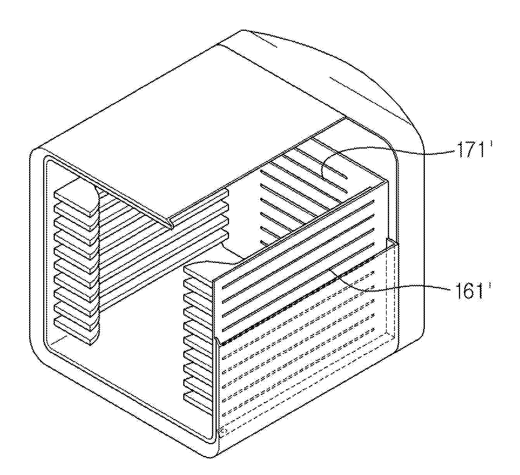
[0061]FIG. 3 is a perspective view of a wafer storage container according to the first exemplary embodiment of the present invention; FIG. 4 is a plan view of FIG. 3; FIG. 5 is a plan view of a wafer storage container according to the second exemplary embodiment of the present invention; FIG. 6 is a plan view of a wafer storage container according to the third exemplary embodiment of the present invention; FIG. 7 is an exploded view illustrating the changes in the areas of the apertures of the holes in FIGS. 3 to 6; FIG. 8 is a perspective view illustrating another type of the holes in FIG. 3; FIG. 9 is an exploded view illustrating the changes in the lengths of the holes in FIG. 8; FIG. 10 is an exploded view illustrating the pipes installed in the holes of a separating wall; FIG. 11 is a perspective view illustrating the 1-1 exemplary...


PUM


Abstract

The present invention relates to a wafer storage container, more particularly, relates to a wafer storage container wherein the space of the wafer storage container is divided into the spaces, namely a storage room, a gas injection room, and a gas exhausting room, which are independent and separate from each other, so when the wafer storage container is transported to the load port and being coupled therewith, the purge gas is injected / exhausted through the separating walls inside the storage room, thereby efficiently removing the remaining fumes on the surface of the wafer.

Description

CROSS-REFERENCE TO RELATED APPLICATION[0001]This application claims priority to and the benefit of Korean Patent Application No. 10-2015-0040523 filed on Mar. 24, 2015, the disclosure of which is incorporated herein by reference in its entirety.FIELD OF INVENTION[0002]The present invention relates to a wafer storage container, more particularly, relates to a wafer storage container for efficiently removing residual fumes remaining on the wafer surface by injecting purge gas.BACKGROUND[0003]Generally, semiconductor devices are manufactured by selectively and repeatedly performing processes such as vacuum deposition, polishing, photolithography, ion injection, cleaning, inspection, thermal treatment, and the like on the semiconductor wafers; and the wafers are transported to a specific location required for each process in order to be formed as semiconductor devices.[0004]During the semiconductor manufacturing process, the wafers being processed are products of high precision, and the...

Claims


Application Information

Patent Timeline
Patent Type & Authority Applications(United States)
IPC IPC(8): H01L21/673
CPCH01L21/67389H01L21/67393
Inventor WOO, BUM JEYOON, SEOK MUNHAN, MYOUNG SOKKIM, HYUN SIN
Owner PICO & TERA CO LTD
Why Eureka
Try Eureka